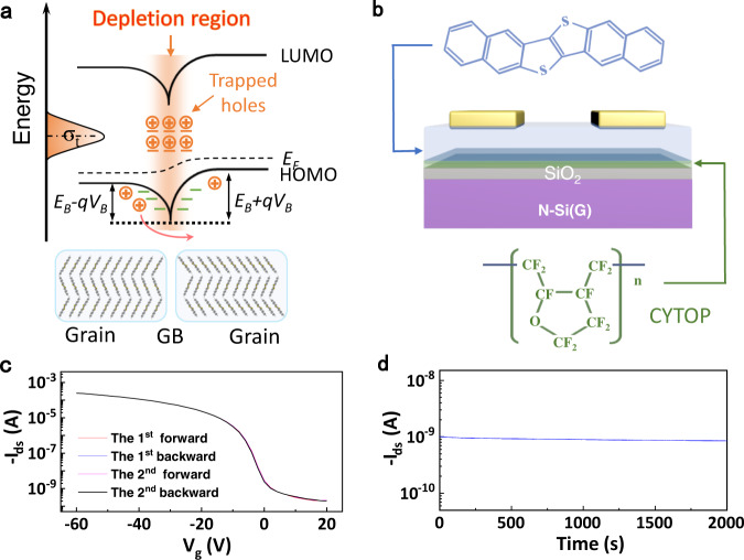
Fig. 1. Energy band diagram, OFET structure and operational stability data.
a Schematic diagrams of energy band model at grain boundary (GB) of polycrystalline semiconductor with a bias voltage. b Schematic illustration of OFET and molecular structure of DNTT and CYTOP. c OFET transfer curves during the two cycle tests. Vds = −60 V. d Bias stress curve of the OFET. Vgs = 0 V, and Vds = −60 V. The data in (c, d) denote the excellent operational stability of DNTT OFET.

