
Fig. 3. Directional transport along defects.
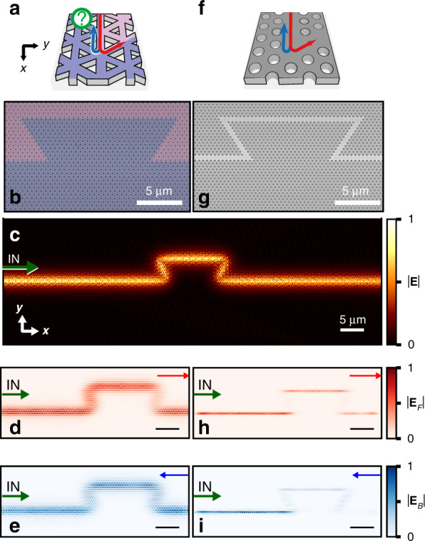
For the topologically non-trivial VPC waveguide, a shows the schematic of the probed 120° corner. b Top-view SEM image of the fabricated Ω-shaped defect. Two-dimensional real-space amplitude maps showing the c, full mode amplitude distribution, d forward-propagating mode amplitude only, and e backward-propagating mode amplitude only. The amplitude maps are normalized independently to their maximum value. For a topologically trivial W1 waveguide, f schematically shows the mode propagation around a 120° corner, and g shows a top-view SEM image of the device. The two-dimensional amplitude maps of the filtered forward- and backward-propagating modes are shown in h and i, respectively. The direction of in-coupling is indicated by the green arrows. All scale bars correspond to 5 μm