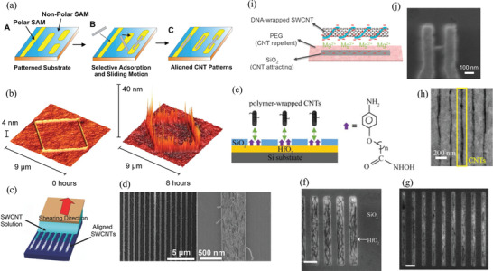
Figure 5.

a) Figure depicting adhesion of CNTs onto polar hydrophilic patterned SAM on substrates, followed by “sliding” of CNTs protruding on hydrophobic regions toward hydrophilic regions. Reproduced with permission.[ 118e ] Copyright 2006, AIP Publishing. b) AFM image of Si substrate patterned by etching an SAM resist through probe lithography, and then subsequent amide attachment of CNTs to the patterned area. Reproduced with permission.[ 118h ] Copyright 2007, Elsevier. c) SWCNT solution shearing over nanoscale SAM patterned substrate. d) Scanning electron microscope (SEM) images of nanoscale, aligned SWCNT lines patterned using the technique. Reproduced with permission.[ 110j ] Copyright 2015, Wiley‐VCH. e) Polyfluorene‐sorted semiconducting SWCNTs deposited via complexation with diazonium head group on SAM attached to HfO2 regions. SEM images of SWCNTs patterned inside f) 100 nm and g) 50 nm wide trenches, and h) SWCNTs that were deposited in the 50 nm trenches after etching of SiO2. Reproduced with permission.[ 133 ] Copyright 2017, American Chemical Society. i) DNA‐wrapped semiconducting SWCNTs attracted to hydrophilic SiO2 patterned regions mediated by a magnesium ion charge inversion layer. j) SEM image of a single SWCNT CNTFET fabricated with the patterning technique. Reproduced with permission.[ 126c ] Copyright 2016, American Chemical Society.
