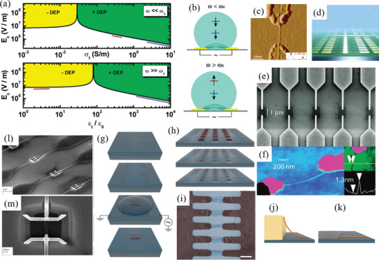
Figure 7.

a) Example plots depicting DEP regimes for SWCNTs in 0.1% sodium dodecylbenzenesulfonate surfactant aqueous suspension. For low‐frequency AC DEP (top), conductivity and electric field strength determine whether CNTs are attracted (green, + DEP) or repelled (yellow, – DEP) from the electrodes. For high‐frequency AC DEP (bottom), relative permittivity (dielectric constant) and electric field strength determine attraction (green, + DEP) or repulsion (yellow, – DEP) from the electrodes. b) In this example, values of conductivity/relative permittivity of metallic (blue) and semiconducting (red) SWCNTs mostly result in attraction to the electrodes except for semiconducting SWCNTs in the high‐frequency regime. Note that this plot only represents values for a specific example and different solvents, dispersing agents, and CNTs will change these values. Reproduced with permission.[ 146 ] Copyright 2004, American Chemical Society. c) AFM image of a single individualized SWCNT deposited across Ag electrodes with inset showing topography over the deposited SWCNT. Scale bar 100 nm. Reproduced with permission.[ 156 ] Copyright 2003, American Chemical Society. d) Schematic of DEP CNT patterning for fabrication of high‐density CNT device array. e) SEM image and f) AFM images of fabricated single CNT devices. Reproduced with permission.[ 2a ] Copyright 2007, American Chemical Society. g) Schematic depicting DEP patterning of CNTs on graphene electrodes and subsequent etching of the graphene. h) The nanoscale DEP patterning technique can pattern different nanomaterials between removable electrodes over whole wafers. i) AFM image of deposited CNTs between graphene electrodes with nanoscale precision. Scale bar 1 µm. j) Curved deposition of CNTs on metal electrodes and k) flat deposition of CNTs on graphene electrodes. Reproduced under the terms of the CC BY 4.0 license.[ 164c ] Copyright 2005, The Authors, published by Elsevier. l) Array of nanoscale‐suspended SWCNT devices fabricated via DEP patterning. Scale bar 2 µm. m) Suspended SWCNT device with only two parallel SWCNTs suspended between the electrodes. Scale bar 200 nm. Reproduced with permission.[ 183 ] Copyright 2015, Wiley‐VCH.
