
Figure 20.
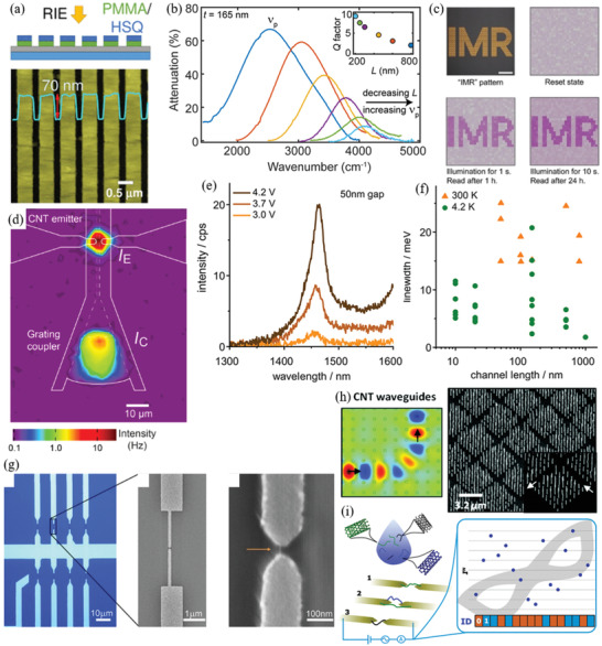
a) Illustration and AFM image of highly aligned SWCNT film cut into nanoscale stripes using oxidation etching through an EBL patterned resist. b) Attenuation due to coherent plasmon resonance in nanoscale patterned SWCNT films. Decreasing SWCNT lengths from 800 to 200 nm results in increasing peak wavenumber. Reproduced with permission.[ 216i ] Copyright 2017, American Chemical Society. c) Flexible CNT device incorporating both photodetection and memory applications fabricated by oxidation etching. The device can store sensed images in memory for up to 24 h after only 10 s exposure. Reproduced with permission.[ 216k ] Copyright 2020, Wiley‐VCH. d) Spatially resolved light emission of a CNT transducer device fabricated by DEP CNT patterning. Strong and stable emission is observed from the SWCNTs bridging the electrodes coupled with a waveguide. Reproduced under the terms of CC BY 4.0 license.[ 395a ] Copyright 2017, The Authors, published by Beilstein‐Institut. e) Typical electroluminescence spectra of individual (9,8) SWCNT devices with short channels at room temperature. 50 nm channel (gap) is presented at varying bias voltages. f) Peak full‐width at half‐maximum for varying channel lengths at room and cryogenic temperatures. g) Optical (left) and SEM image (middle) of the devices and SEM image (right) of a (9,8) SWCNT deposited via DEP between electrodes in the device. Reproduced with permission.[ 396 ] Copyright 2020, American Chemical Society. h) Vertical CNT array waveguide metamaterial fabricated by EBL patterning of CNT growth catalyst and subsequent CVD growth. Reproduced with permission.[ 398 ] Copyright 2011, American Chemical Society. i) Heterogenous mixture of CNTs can be patterned by DEP CNT patterning onto a device to produce randomly generated resistances for each device. These resistances can be read as a physically unclonable function for cryptographic identification. Reproduced with permission.[ 401b ] Copyright 2019, American Chemical Society.