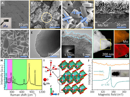
Fig. 2. Morphological and structural characterization of the MoOx electrode.

(A and B) SEM images of (A) the polished Mo foil and (B) SEM image of the MoOx electrode. (C) Cross-sectional SEM images of MoOx electrode. (D) SEM images of the contact surface between MoOx flakes and inner Mo foil. (E and F) TEM and high-resolution TEM (HRTEM) images of the delaminated MoOx flakes, respectively. The inset in (F) shows the corresponding selected-area electron diffraction (SAED) pattern. (G) Acquired energy-dispersive spectroscopy (EDS) elemental mapping of MoOx flakes. (H) Raman spectrum of MoOx electrodes. a.u., arbitrary unit. (I) Crystal structure of α-MoO3, representing the layered structure and three types of oxygen anion. (J) ESR spectra of MoOx and MoO3. Inset: Digital photographs of MoOx (left) and MoO3 (right) powders. Photo credit: Hongwei Sheng, Lanzhou University.
