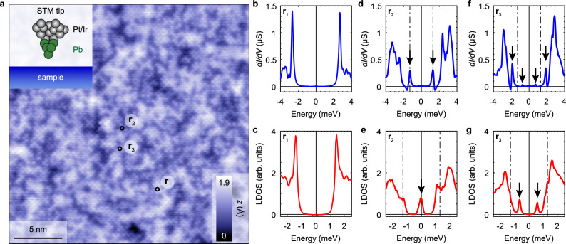
Fig. 1. Scanning Tunneling Microscopy on FeTe0.55Se0.45 with a superconducting tip.
a Atomically resolved topographic image (z-height map, 25 × 25 nm2) of FeTe0.55Se0.45 cleaved surface acquired with a Pb coated Pt/Ir tip (see inset) at 2.2 K in ultra-high vacuum. Setup condition: Vset = −8 mV, Iset = −100 pA. b, d, f Spatially averaged differential conductance spectra in the areas (r1, r2, r3) marked by the black circles in a. r1: no in-gap states. r2: two in-gap resonances at ± 1.3 meV. r3: two sets of peaks symmetric in energy around the Fermi level. c, e, g Deconvolution of the spectra shown in b, d, f, respectively, provide information about the intrinsic LDOS of the sample in the indicated areas. In r2 a zero-bias impurity state is recovered and in r3 two in-gap states are observed. Setup conditions: b Vset = 6 mV, Iset = 1.2 nA, d, f Vset = 5 mV, Iset = 2 nA. Lock-in modulation is μV peak-to-peak for all measured spectra.

