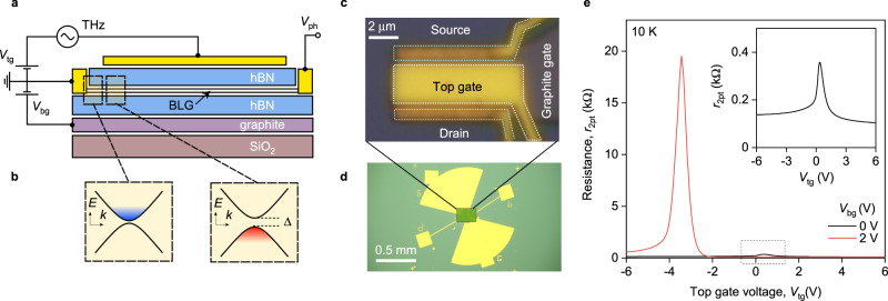
Fig. 1. Dual-gated bilayer graphene THz detector.
a Schematic of an hBN encapsulated dual-gated BLG transistor. THz radiation is incident on a broadband antenna connected to the source (S) and gate terminals yielding modulation of the top gate-to-source voltage (Vtg) while the back gate voltage (Vbg) is fixed. The build-up photovoltage Vph is read out between the source and drain (D) terminals. b Band structure of the BLG at the interface between the n-doped bottom gate-sensitive region and dual-gated p-doped channel (Δ is the induced band gap). Blue and red colours illustrate conduction and valence bands fillings, respectively. Note, even for a single-gated region, a finite band gap appears in the energy dispersion due to the difference in on-site energies between the top and bottom graphene layers44. c, d Optical photographs of the fabricated dual-gated detector. The source and top-gate terminals are connected to a broadband bow-tie antenna. e The two-terminal resistance of our BLG device, r2pt, as a function of Vtg for two representative Vbg = 0 and Vbg = 2 V. Inset: Zoomed-in r2pt(Vtg) for Vbg = 0 V. T = 10 K.

