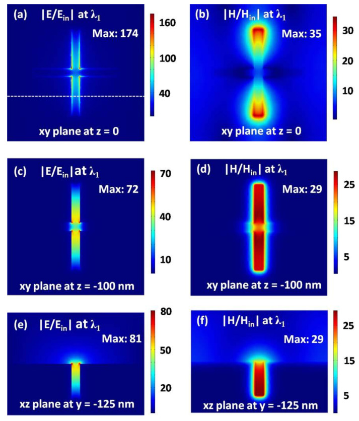
Figure 3.
Electric (a,c,e) and magnetic (b,d,f) field strength at the resonance wavelength of λ1. The xy plane with z = 0 (a,b) is just on the top surface of the metal substrate. The xy plane with z = −100 nm (c,d) is at the geometrical center of the cross-shaped hole. The xz plane with y = −125 nm (e,f) is along the white dotted line in (a).

