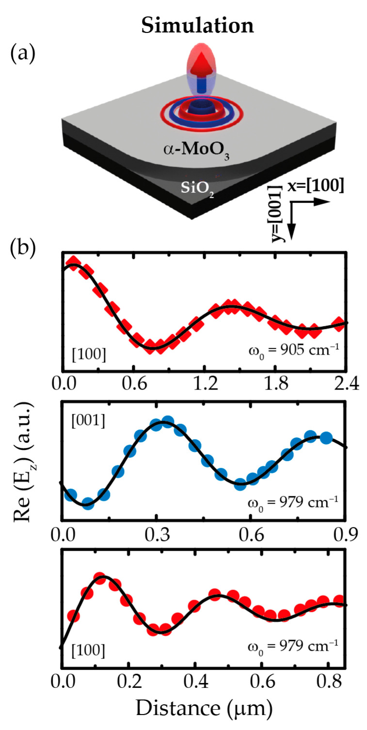
Figure 3.
(a) Schematics of a 225-nm-thick α-MoO3 slab on a SiO2 substrate in which propagating PhPs are depicted by elliptical fringes (represented in red and blue). A vertically oriented electric point dipole placed on top of the structure provides concentrated electric fields that allow for launching PhPs at an incident wavelength 979 cm−1 (elliptic regime). (b) Simulated electric field profiles (dots), Re(Ez), along the [100] and [001] crystal directions of α-MoO3 for an incident frequency 905 cm−1 (hyperbolic regime) and 979 cm−1 (elliptic regime). The fit to the simulated profiles are depicted with a black solid line.

