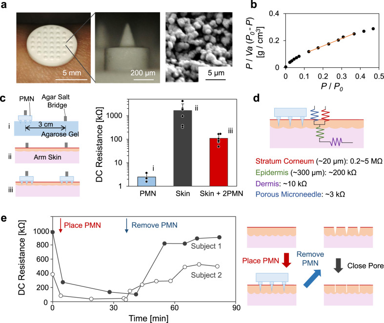
Fig. 2. Structural and electrical characterization of porous microneedles (PMN).
a Representative photographs of a chip of PMN arrays and a representative cross-sectional SEM image of PMN (N = 3 independent samples). b A BET plot for nitrogen adsorption in PMN. Vα [cm3/g] is the adsorbed gas volume per the weight of PMN at STP. P and P0 are the monitored and the saturation pressure [Pa], respectively. c The DC resistance of (i) a PMN (N = 3 independent experiments; mean ± standard deviation (SD)), (ii) human arm skin (N = 6 independent experiments for 3 human subjects; mean ± SD), and (iii) the skin with PMNs (N = 6 independent experiments for 3 human subjects; mean ± SD), measured by applying 1 µA. d Schematic of the equivalent DC circuit of a layered structure of a skin with the experimental resistances of each layer. e The time-course of DC resistance of two human subjects’ arm skin, in which the red arrow and the blue arrow indicate the timing when the PMN was placed and removed, respectively. During the period of PMN insertion, a tubular salt-bridge was put on the PMN as in (c-iii). Right illustration draws the pore closure after the removal of PMN.

