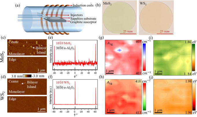
Fig. 1. Monolayer film growth and characterization.
a Schematic of the MOCVD system with a cold-wall horizontal reactor. b 2″ sapphire wafer with MOCVD grown MoS2 and WS2. AFM images of c MoS2 and d WS2 at the center and edge of the respective wafers. Towards the center of the MoS2 film, few bilayers are seen. In-plane XRD ϕ-scan of e MoS2 and f WS2 on sapphire (α-Al2O3), showing the epitaxial relationship between the monolayers and the sapphire substrate. Raman map of the A1g peak position for g MoS2 and h WS2 films transferred from the growth substrate onto the device fabrication substrate with 50 nm ALD Al2O3. Low variation in the peak position is observed for both MoS2 and WS2 with an average of ≈403.5 cm−1 and ≈417 cm−1, respectively. PL peak map of i MoS2 with an average of ≈1.85 eV and j WS2 with an average of ≈1.97 eV, confirm monolayer films. PL is a characteristic of monolayer film owing to indirect to direct bandgap transition.

