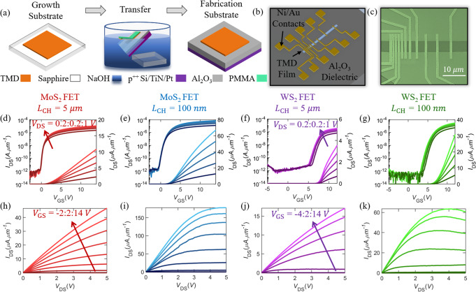
Fig. 2. Device fabrication and electrical measurements.
a Schematic representation of PMMA-assisted wet transfer of monolayer TMD films from sapphire (growth substrate) to an Al2O3 substrate. b Schematic representation and c SEM of a TLM structure defined using e-beam lithography. TLM structures with channel length (LCH) from 100 nm to 5 μm are fabricated and the channel width is defined to be 5 μm. Transfer characteristics, i.e., drain current (IDS) versus gate voltage (VGS), for different drain voltages (VDS) in logarithmic and linear scale for d longest-channel (LCH = 5 μm) and e shortest-channel (LCH = 100 nm) MoS2 field-effect transistors (FETs), and f longest-channel (LCH = 5 μm) and g shortest-channel (LCH = 100 nm) WS2 FETs. Corresponding output characteristics, i.e., IDS versus VDS, for different VGS for h longest-channel and i shortest-channel MoS2 FETs, and j longest-channel and k shortest-channel WS2 FETs.

