Fig. 4.
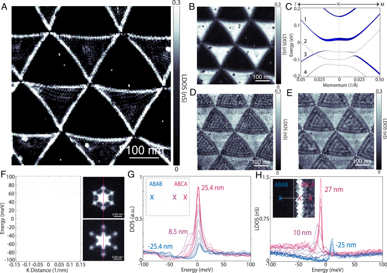
Gate-tunable topological edge states ABCA graphene. (A and B) STS LDOS map cuts at −20 meV (within the overlapping gap of ABAB and ABCA graphene) and −10 meV (at the flat-band edge peak). (C) Band structure of ABAB graphene at a displacement field of 0.8 V/nm as calculated by DFT with self-consistent charge screening. The size of the blue circles is proportional to the projection of the wavefunction on the top layer. (D and E) STS LDOS map cuts (from same map as A and B) at 37.5 and 22.5 meV. (F) Two-dimensional Fourier transform of D and E (Right) and a linecut through the primary electron scattering peaks (Left). (G) Tight-binding LDOS profiles at fixed spatial intervals crossing an ABAB–ABCA domain wall with their corresponding distances (with respect to the domain boundary) color coded and written for the beginning and end point as well as the dominant in-gap topological edge state. (H) STS LDOS profiles at fixed spatial intervals crossing the ABAB–ABCA domain wall at the represented and color-encoded distances (with respect to the domain wall as determined at higher energies) showing the dominant in gap topological edge state about 10 nm into the ABCA domain, consistent with tight binding in G. STS measurements in A, B, D, E, and H were taken at setpoints of 400 mV and 150 pA with lock-in oscillations of 2.5 mV (A, B, D, and E) and 1 mV (H).

