Figure 2.
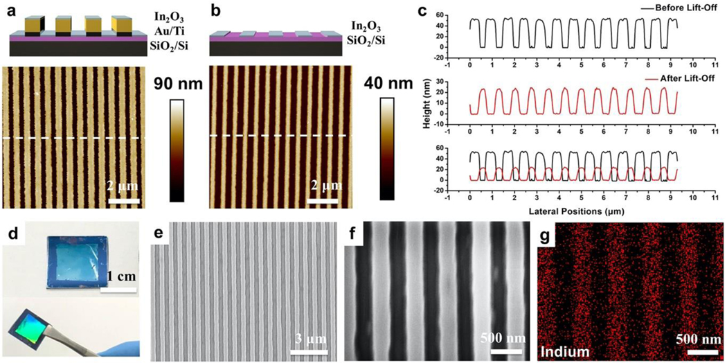
Atomic force microscope (AFM) images of 350-nm nanoribbon substrates (a) before (Step 5, Figure 1) and (b) after removing underlying Au structures (Step 6, Figure 1). (c) Height profiles from the AFM images in (a) and (b) across the nanoribbons. (d) Photographs of In2O3 nanoribbons at different viewing angles. (e,f) Scanning electron microscope (SEM) images of 350-nm-wide In2O3 nanoribbons. (g) Energy-dispersive X-ray mapping of indium corresponding to the SEM image in (f).

