

Abstract

The crystallographic orientation control of GaN nanowires (NWs) has been widely investigated by varying the V–III ratio. Here, we report the tuning of crystallographic orientation of GaN NWs by varying the composition of indium (In) in gallium–gold (Ga–Au) alloy catalyst using metal–organic chemical vapor deposition (MOCVD). The c-plane GaN thin film and sapphire substrate are used as growth templates. We found that the substrates of same orientation have a negligible influence on the orientation of the GaN NWs. The catalyst composition and the dimensions of alloy droplets determine the morphology of the NWs. The density of the NWs was controlled by tuning the droplet size of the alloy catalysts. With the constant V/III ratio, the crystallographic orientation of the GaN NWs was tuned from m- to c-axis by increasing the In composition inside alloy catalyst.
1. Introduction
The III–V nanowires (NWs) have excellent electrical and optical properties and allow varying designable structures and devices when combined with heterostructures.1−3 These NWs with excellent performance have a critical role in nanoscale optoelectronic and electronic devices such as light-emitting diodes (LEDs),4−6 laser diodes,7 piezoelectric nanogenerators,8−10 and solar cells.11 In the case of bulk materials, the factor of lattice mismatch limits the combination of materials having different crystal parameters. However, owing to the small dimensions and the nature of freestanding growth, the NWs have the ability to accommodate large lattice mismatch and to grow on materials with different crystal parameters.12 Regarding the growth of NWs, a variety of growth processes are available, such as vapor–solid–solid,13 solid–liquid–solid,14,15 supercritical-fluid–liquid–solid,16 vapor-adsorption-layer–solid,17 and vapor–liquid–solid (VLS).18 The most common mechanism adopted for the growth of III–V NWs is the VLS growth mechanism.19,20 A series of devices and materials such as thermal transport, photonics, and electronics have been developed by VLS growth, but plenty of challenges remain to grow the desirable structures. The parameter window in terms of pressure, temperature, or V/III ratio is very narrow for growing the desired crystallographic orientation. To achieve the desired structure, the understanding of the fundamental growth mechanism is very important.
Wagner et al. discovered the VLS mechanism for the growth of NWs, in which a metal nanoparticle is required to assist the NW growth.18 The role of the metal nanoparticle is to lower the activation energy barrier by catalyzing the pyrolysis of precursors, and because of this reason, the growth rate of metal-assisted nanowires is higher than the growth rate of thin films.21 In this study, we emphasized the agglomeration of metal nanoparticles as well as their effect in shaping the NWs.
Researchers investigated a variety of metals such as Fe, Ni, In, Pt, and Au to optimize the VLS growth of GaN NWs.22−25 Au is the most common due to its ability to form low-melting eutectics with most of the semiconductor components such as Au–Si, Au–In, and Au–Ga. However, several discrepancies are found in the preliminary reports regarding the catalyst-assisted growth of GaN NWs. Zhang et al. investigated the impact of different metals on the growth of GaN NWs and observed that GaN NWs were not grown when Au was used as a metal catalyst.26 Unfortunately, the important concept behind the VLS growth mechanism is not emphasized, and because of that reason, the understanding of detailed process is complicated. It is a real fact that the growth of NWs can be optimized using different metal catalysts with the careful investigation of agglomeration behavior of liquid metal droplets. Change in crystallographic orientation has been attributed to the choice of substrate or change in the V–III ratio.27,28 To the best of our knowledge, there are a few reports on the crystallographic orientation control of NWs by varying the catalyst composition.29,30 Kuykendall et al. achieved the selective growth of GaN NWs along two nonpolar directions by adjusting the ratio of gold to nickel in the catalyst.29 Regarding the crystallographic orientation of the NWs, Joyce et al. proposed a model to control the crystallographic orientation of the GaN NWs by varying the temperature and V/III ratio.31 In the VLS growth mechanism, the solidification process starts by the formation of two-dimensional nuclei at alloy droplet–crystal interface31,32 originating from triple-phase-boundary (TPB) line such as vapor–liquid–solid boundary33 depending upon the crystal structure and surface energies of facets.34 Because of the negligible solubility of nitrogen in Au, the TPB line is the preferred site for the formation of two-dimensional nucleation.35 Generally, the fundamental concepts for the growth of crystalline solids using any phase system are supersaturation, preferred deposition, and nucleation.33 The challenging aspect for the crystal growth is the understanding of the transient and dynamic nucleation process. The optimization of growth conditions facilitates finding the probability of nucleation on the surface of substrate.
In this study, we investigated the agglomeration behavior of Ga–Au and In–Ga–Au alloy droplets at different agglomeration temperatures and their consequent effect on the growth of GaN NWs. In VLS growth, the alloy droplet is the preferred site for the vapors, which cause the droplet to be supersaturated. The shape and size of alloy droplets have a major influence on the growth of nanowires. Overall, the crystallographic orientations of the NWs depend on the specific orientation of liquid–crystal interface, which is defined by the crystal facet for which the interfacial energy is suitable. This interfacial energy is dependent on the surface energies of alloy droplet and crystal. With the growth of NWs, the droplet–crystal interface keeps moving along the growth direction and the control of specific crystallographic orientation is entirely dependent on the growth parameters. The movement of droplet–crystal interface is dependent on the minimization of interfacial energy; in that sense, the lowest-energy facets will grow faster. As per the Ga–Au36 and In–Ga–Au37 phase diagrams, the calculated Ga, In, or Au composition inside the alloy as a function of temperature helps in starting nucleation at the desired crystallographic facet of material. Unfortunately, at high temperatures, the experimental investigation of different facets energies of alloy is not an easy task.
In this study, we optimized the growth of GaN NWs using Ga–Au and In–Ga–Au alloy catalyst. We utilized the Au-coated c-plane GaN TF (will be referred to as GaN substrate) and Au-coated sapphire substrates for the growth of GaN NWs. Prior to the growth of GaN NWs, the agglomeration behavior of Ga–Au and In–Ga–Au alloy catalysts on both the substrates was investigated at different agglomeration temperatures. We tuned the droplet size by changing the In and Au composition inside the droplets and by agglomerating the alloy at different temperatures. The Ga composition was fixed in both the Ga–Au and In–Ga–Au alloy catalysts, whereas the shape, diameter, and density of NWs were found to be different depending upon the agglomeration temperature and TMIn composition.
2. Experimental Section
Two experimental strategies were employed; the agglomeration behavior was investigated first for In–Ga–Au (with variable In composition) alloy on GaN and sapphire substrates. The second strategy was employed to investigate the consequent effect of agglomeration on the growth of GaN NWs. All of the growth experiments were performed using metal–organic chemical vapor deposition (MOCVD) (CCS-FT 19 × 2 in., Aixtron) with a facility to load nineteen 2-in. wafers in a single experiment. Before starting the experiments in MOCVD, the Au film as a metal catalyst was evaporated on GaN and sapphire substrates with three different thicknesses (1, 5, and 10 Å) using an e-beam evaporator. The GaN samples coated with Au were referred to as G-1, G-5, and G-10, while the sapphire samples coated with Au were referred to as S-1, S-5, and S-10. Depending upon the number of experiments, we prepared several clusters of these six samples (G-1, G-5, G-10, S-1, S-5, S-10) to load each cluster separately before starting a new experiment.
To investigate the agglomeration behavior of the In–Ga–Au alloy catalyst, overall three sets of experiments were performed. In the first set of experiments, the TMIn flow was 0 μmol/min and agglomeration of Ga–Au alloy catalyst is investigated. For the second and third sets of experiments, the TMIn flow was 2.07 and 4.14 μmol/min, respectively. In the further discussion, the first, second, and third sets are referred to as Set-(0)In, Set-(2.07)In, and Set-(4.14)In, respectively (Table 1). In all of the experiments, the trimethylgallium (TMGa) flow and reactor pressure were maintained at 37 μmol/min and 75 Torr. Each set was composed of three experiments depending on agglomeration temperatures such as 650, 750, and 850 °C, as shown in Table 1. To investigate the agglomeration behavior of alloy catalyst, overall nine experiments were performed, which are referred to as Exp-650_Set-(0)In, Exp-750_Set-(0)In, Exp-850_Set-(0)In, Exp-650_Set-(2.07)In, Exp-750_Set-(2.07)In, Exp-850_Set-(2.07)In, Exp-650_Set-(4.14)In, Exp-750_Set-(4.14)In, and Exp-850_Set-(4.14)In.
Table 1. Sequence of Experiments Performed for the Agglomeration of Ga–Au and In–Ga–Au Alloy Droplets at Different Agglomeration Temperatures and Variable In Composition.
| set | experiments | agglomeration temp. (°C) | TMIn (μmol/min) | TMGa (μmol/min) | pressure (Torr) | agglomeration Time (s) |
|---|---|---|---|---|---|---|
| Set-(0)ln | Exp-650 Set-(0)ln | 650 | 0 | 37 | 75 | 900 |
| Exp-750 Set-(0)ln | 750 | |||||
| Exp-850 Set-(0)ln | 850 | |||||
| Set-(2.07)In | Exp-650_Set-(2.07)In | 650 | 2.07 | 37 | 75 | 900 |
| Exp-750_Set-(2.07)In | 750 | |||||
| Exp-850_Set-(2.07)Tn | 850 | |||||
| Set-(4.14)In | Exp-650_Set-(4.14)In | 650 | 4.14 | 37 | 75 | 900 |
| Exp-750_Set-(4.14)In | 750 | |||||
| Exp-850_Set-(4.14)In | 850 |
As mentioned above, before starting each experiment, a new cluster of eight Au-coated samples was loaded into the reactor. The Exp-650_Set-(0)In was performed by loading the first cluster of eight Au-coated samples into the MOCVD reactor. The reactor temperature was gradually ramped up to 600 °C and gallium layer (Ga layer) was deposited by introducing trimethylgallium (TMGa) for 135 s with a flow rate of 37 μmol/min. In the subsequent step, the temperature was ramped up to 650 °C and the agglomeration of Ga and Au layers into the Ga–Au alloy was performed for 900 s (agglomeration time) under the reactor pressure of 75 Torr. For Exp-750_Set-(0)In and Exp-850_Set-(0)In, the agglomeration temperature was ramped up to 750 and 850 °C, respectively; however, all of the other parameters were same.
In Set-(2.07)In of experiments, prior to the deposition of Ga layer, TMIn was introduced at 550 °C with a flow rate of 2.07 μmol/min for 90 s. For Exp-650_Set-(2.07)In, the agglomeration of the In–Ga–Au alloy was performed at 650 °C, while for Exp-750_Set-(2.07)In and Exp-850_Set-(2.07)In, the agglomeration was performed at 750 and 850 °C, respectively. In Set-(4.14)In of experiments, the TMIn flow was increased to 4.14 μmol/min and the agglomeration of In–Ga–Au alloy was performed at the same three agglomeration temperatures as mentioned in Set-(0)In and Set-(2.07)In of experiments.
The second experimental strategy was implemented by performing the sequential growth of GaN NWs using all of the above-mentioned agglomeration conditions. For the agglomeration conditions of Exp-650_Set-(0)In and Exp-750_Set-(0)In, the growth of GaN NWs was performed at 750 °C, for the agglomeration conditions of all other experiments, the NWs were grown at 850 °C. The reason for this selection is discussed with details in the Results and Discussion section. The growth of GaN NWs was performed in the H2 environment by introducing TMGa and NH3 with fixed flow rates of 37 μmol/min and 4.9 mmol/min for 3000 s, respectively, under the reactor pressure of 60 Torr.
The morphological analysis of alloy catalyst and NWs was performed by secondary electron microscopy (SEM). To confirm the composition of metals inside the In–Ga–Au alloy catalyst, the SEM–energy-dispersive spectroscopy (SEM–EDS) analysis was performed. The single crystallinity and crystallographic orientation of NWs were confirmed by transmission electron microscopy (TEM). The elemental mapping of catalyst atop of single NW was performed by TEM–EDS.
3. Results and Discussion
In the VLS growth mechanism, the role of metal catalyst is to lower the activation energy barrier by catalyzing the pyrolysis of precursors. Before nucleation, the growth species dissolve in agglomerated alloy droplet and form the supersaturated solution. The growth species can reach the droplet directly from vapor phase and by diffusion from the substrate surface. Once the alloy droplet gets supersaturated with respect to the droplet–crystal interface, the crystal growth is initiated. Supersaturation is a common term mostly used in continuum studies for alloy droplet to initiate nucleation at droplet–crystal interface; however, this term is misleading if not compared with the saturation level of other phases. The VLS growth is a three-phase system, and the alloy droplet is the liquid phase and has a large accommodation coefficient; if it is supersaturated with respect to vapor phase, no more accommodation will take place followed by the desorption of growth species back to vapor phase. To start the nucleation at the droplet–crystal interface, the chemical potential of alloy droplet should be in between the chemical potentials of vapor and solid phases, i.e., lower than alloy droplet and higher than solid.
Overall, the NW growth process involves the complicated thermodynamics and depends on several parameters such as type of metal catalyst, type of growth substrate, carrier gas (H2 or N2), Ga vapor pressure, V/III ratio, reactor pressure, and growth temperature. It is very difficult to investigate the influence of each parameter individually. We fixed several optimal growth parameters such as metal catalyst, carrier gas, V/III ratio, TMGa flow, reactor pressure, and varied composition of metals such as Au and In in alloy droplet and agglomeration temperature of alloy and investigated their subsequent effect on the growth of GaN NWs.
Prior to the growth of GaN NWs, the agglomeration behavior of In–Ga–Au alloy catalyst was investigated on both the substrates (GaN and sapphire) at different agglomeration temperatures of 650, 750, and 850 °C. Based on the content of this study, we divided the discussion into two parts. In the first part, we discussed the Set-(0)In of experiments, in which TMIn flow was 0 μmol/min and the catalyst is composed of Ga–Au alloy. Then, the growth of GaN NWs is performed using the agglomeration conditions of each experiment performed in Set-(0)In. In the second part, we discussed the agglomeration behavior of In–Ga–Au alloy droplets with variable In composition followed by their consequent effect on the growth of GaN NWs.
3.1. Ga–Au Alloy Catalyst
In the first experiment (Exp-650_Set-(0)In) of Set-(0)In, the agglomeration of the Ga–Au alloy catalyst was performed at 650 °C (Figure 1a), while in the second (Exp-750_Set-(0)In) and third experiments (Exp-850_Set-(0)In) of Set-(0)In, the agglomeration was performed at 750 and 850 °C, respectively (Figure 1b,c).
Figure 1.

Agglomeration of Ga–Au alloy agglomerated at 650 °C on (a-i) GaN and (a-ii) sapphire substrates, Ga–Au alloy droplets agglomerated at 750 °C on (b-i) GaN and (b-ii) sapphire substrates, Ga–Au alloy droplets agglomerated at 850 °C on (c-i) GaN and (c-ii) sapphire substrates. All of the scale bars are for 100 nm.
For Exp-650_Set-(0)In, the well-separated Ga–Au alloy droplets are observed on GaN and sapphire substrates coated with a thinner Au film (1 Å). However, the samples coated with thicker Au films (5 and 10 Å) have irregular alloy droplets. To understand this behavior, the agglomeration of the 10 Å thick Au film was performed at 650 °C on GaN and sapphire substrates without adding In and Ga composition; the agglomerated Au film exhibited irregular Au islands instead of droplets (Figure S1a,b). For the tailoring of irregular Au islands to spherical droplets, the agglomeration temperature was enhanced for the next experiments such as Exp-750_Set-(0)In and Exp-850_Set-(0)In. Based on the phase diagram of Ga–Au alloy,36 the melting temperature is low for high Ga composition or for low Au composition. In other words, the Ga–Au alloy with high Au composition requires a high temperature for proper agglomeration; therefore, at a lower agglomeration temperature (650 °C), the agglomerated droplets of 10 Å thick Au films have irregular shapes, as demonstrated in Figure 1a. Moreover, it is clarified that the agglomeration temperature such as 650 °C is not the real temperature on the surface of substrates inside the reactor; it is slightly lower, which is unknown.
For Exp-750_Set-(0)In, the substrates coated with 1 and 5 Å thick Au films exhibited well-separated Ga–Au alloy droplets, as shown in Figure 1b. By performing the agglomeration at 650 and 750 °C, the substrate effect on the agglomeration behavior of alloy droplets was very low and we did not include it in discussion. In the case of the 10 Å thick Au film, still the agglomerated droplets did not exhibit the spherical shape, as shown in the insets (with red border) of Figure 1b(i),(ii). This confirms that for proper agglomeration of the 10 Å thick Au film with given Ga composition, the agglomeration temperature must be enhanced.
In Exp-850_Set-(0)In, the agglomeration temperature was further enhanced to 850 and the 10 Å thick Au film exhibited proper agglomeration (Figure 1c). In this case, the substrate effect on agglomeration of alloy droplets became prominent and the density of Ga–Au alloy droplets on GaN substrate became significantly larger than that on the sapphire substrate; this happened only when agglomeration was performed at 850 °C. This is because of possible decomposition of GaN from top surface, which produces the extra Ga liquid from the GaN surface. The decomposition reduces the diffusion length of Ga adatoms, and because of this reason, the density of alloy droplets on the GaN surface is high. As explained in the Experimental Section, the agglomeration was performed in H2 environment. There is ample evidence that the GaN decomposes from top surface when annealed in H2 environment without flow of N2 and NH3.38 This effect is significant when agglomeration was performed at 850 °C (Figure 1c(i)). In case of sapphire substrate, there is no possibility of surface decomposition, only Ga from TMGa supply combines with Au and forms Ga–Au alloy. Moreover, the diffusion length of Ga adatoms on sapphire surface is rather larger compared with that on GaN surface. Because of the large diffusion length of Ga adatoms on sapphire surface, more adatoms diffuse from the surroundings and coalesce with the Ga–Au alloy droplet, and consequently the density of Ga–Au alloy droplets decreases as a function of agglomeration time and the size of the droplet increases. For Exp-850_Set-(0)In, the average diameter of the Ga–Au alloy droplet on GaN substrate was 46 nm (Au film thickness, 1 Å), whereas it was 53 and 60 nm for Au films with thicknesses of 5 and 10 Å, respectively, as shown in Figure 1c(i). Here, the enhanced diameter of alloy droplets for thicker Au film confirms the proper agglomeration. In the case of sapphire substrate, the average diameters of the Ga–Au alloy droplets from thinner to thicker Au films were 50, 60, and 70 nm, respectively, as shown in Figure 1c(ii). The enhancement in diameters of alloy droplets confirms the larger diffusion length of Ga adatoms on the surface of sapphire.
For the agglomeration conditions of Exp-650_Set-(0)In and Exp-750_Set-(0)In, the growth of GaN NWs was optimized at 750 °C, whereas for Exp-850_Set-(0)In, the agglomeration temperature was 850 °C, so the growth of NWs was performed at the same temperature. In the case of Exp-650_Set-(0)In, the proper agglomeration of Ga–Au alloy droplets was observed on GaN and sapphire substrates coated with a 1 Å thick Au film, as explained above. Using the agglomeration conditions of Exp-650_Set-(0)In, the NWs were grown on the GaN and sapphire substrates only coated with a 1 Å thick Au film because of proper agglomeration. Compared with the NWs grown on the sapphire substrate, the NWs grown on GaN substrate exhibited a relatively high density, but their morphology was very rough (Figure 2a). The magnified image with the red border in Figure 2a shows the rough NWs and droplets on the GaN surface, which confirms that the nucleation was not started from all of the droplets. Similarly, under the same conditions, only a few NWs were grown on sapphire substrates with a high density of the islands (Figure S2a). The diameter of the NWs is relatively larger than the average diameter of the alloy droplets. This is because of the difference between the agglomeration temperature (650 °C) of Ga–Au alloy and the growth temperature (750 °C) of the NWs. Subsequent to the agglomeration performed at 650 °C, the temperature was ramped up to 750 °C in 100 s to initiate the growth. During the ramp-up period, the size of the Ga–Au alloy droplets was slightly increased, which is confirmed from the diameter of the NWs. Additionally, after the supply of growth species, the alloy droplets consumed some time to get supersaturated (depending on their size and V/III ratio), and this time should also be considered in agglomeration because it can also enhance the droplet size. From the SEM images, it seems most of the alloy droplets coalesced with each other during the time of nucleation and the NWs emerged from few droplets only. For the same agglomeration conditions, the NWs were not grown on the substrates coated with 5 and 10 Å thick Au films because the agglomeration was not uniform due to lower agglomeration temperature (as explained in the agglomeration part).
Figure 2.

Growth of GaN NWs on (a) GaN substrate using agglomeration conditions of Set-(0)In-650, on (b-i) GaN and (b-ii) sapphire substrates using agglomeration conditions of Set-(0)In-750, and on (c) sapphire substrate using agglomeration conditions of Set-(0)In-850.
Using the agglomeration conditions of Exp-750_Set-(0)In, the NWs were grown on both the substrates coated with 1 and 5 Å thick Au films. The NWs grown on the GaN substrate are better in morphology compared with the NWs grown on sapphire substrates, as shown in Figure 2b(i),(ii). In addition, in the case of GaN substrate, the NWs grown using the 5 Å thick Au film have a relatively large diameter with circular shape, but the NWs exhibited the lower growth rate compared with the NWs grown using the 1 Å thick Au film; the reason is that the larger droplets consume more growth species than the smaller droplets. Moreover, the NWs grown on GaN using the 1 Å thick Au film are slightly tapered in shape. This is attributed to the lower Au composition inside the Ga–Au alloy droplet. For thinner Au film, at high temperatures, the partial pressure of “Ga” inside the Ga–Au alloy droplets increases; this phenomenon enhances the instability inside the droplets and the excess Ga starts migrating along the sidewall of NWs, while making the tapered shape. In the case of sapphire substrates, the NWs exhibited a low density because of the high diffusion length of Ga adatoms on the sapphire surface. For the same agglomeration conditions, the NWs were not grown on the substrates coated with the 10 Å thick Au film due to irregular agglomeration of Ga–Au alloy droplets, as explained before (in discussion related to agglomeration). In this case, the agglomeration conditions seem to be suitable for the proper agglomeration of Ga–Au alloy droplets on the substrates coated with the 5 Å thick Au film.
In Exp-850_Set-(0)In, the growth temperature was further enhanced to 850 °C, but this time, the NWs were not observed on the substrates coated with 1 and 5 Å thick Au films. As discussed above, for thinner Au films such as 1 and 5 Å, the Ga composition is high (especially in the case of GaN). Based on the phase diagram of the Ga–Au alloy, the agglomeration temperature (850 °C) is not suitable to start nucleation from the droplets with high Ga composition or low Au composition. However, the NW bushes were observed on sapphire substrate coated with the 10 Å thick Au film (Figure 2c). In the case of sapphire substrate, the alloy droplets agglomerated at 850 °C are larger in size (70 nm). With the fixed V/III ratio, the larger alloy droplets consume more time to get supersaturated, which further enhances the droplet size (because of the high diffusion length of Ga atoms on sapphire). During the nucleation process, the large quantity of Ga inside the droplets distributes Au on the surface in different patches because of the high partial pressure of Ga. The nucleation started from the distributed Au particles facilitates the growth of NW bushes. In the case of GaN substrate coated with the 10 Å thick Au film, the surface decomposition of GaN at 850 °C was prominent, and the alloy droplets coalesced with each other to form high-density islands on the surface, as shown in Figure S2b. TEM and selective area electron diffraction (SAED) analyses were performed to confirm the single crystallinity and crystallographic orientation of the GaN NWs grown using agglomeration conditions of Set-(0)In. From the Set-(0)In, the NWs exhibiting the best morphology are selected for TEM characterization. Figure 3a shows the TEM image of single GaN NW grown on GaN substrate using agglomeration conditions of Exp-750_Set-(0)In, and the NWs did not exhibit the smooth surface, as shown in the inset. The lattice fringes are also shown in the inset exhibiting a d-spacing of 0.27 nm, which is consistent with the d-spacing of m-axis GaN NWs. Similarly, the SAED diffraction pattern can be seen in Figure 3b, which reveals that the NWs are single crystalline and grown along the m-axis.
Figure 3.

(a) TEM image of GaN NWs grown on GaN substrate using agglomeration conditions of Exp-750_Set(0)In and (b) SAED diffraction pattern of the same GaN NW.
3.2. In–Ga–Au Alloy Catalyst
As discussed in the Experimental Section, “In” was incorporated in the experiments performed in Set-(2.07)In and Set-(4.14)In with TMIn flow rates of 2.07 and 4.14 μmol/min, respectively. This is the second part of discussion in which the Set-(2.07)In and Set-(4.14)In of experiments are discussed; initially, we discussed the agglomeration behavior of In–Ga–Au alloy at different agglomeration temperatures and then their consequent affect on the growth of NWs is discussed. Figure 4a–c shows the agglomeration of In–Ga–Au alloy performed at 650 °C (Exp-650_Set-(2.07)In), 750 °C (Exp-750_Set-(2.07)In), and 850 °C (Exp-850_Set-(2.07)In), respectively. Overall, the agglomeration behavior of Ga–Au and In–Ga–Au alloy droplets followed the same trend to increase their sizes with an increase in agglomeration temperature, but in the case of In–Ga–Au, the change in size is significant. This attributes to the fast thermal decomposition of TMIn compared with that of TMGa and high surface mobility of In adatoms.39
Figure 4.

Agglomeration of In–Ga–Au alloy agglomerated at 650 °C on (a-i) GaN and (a-ii) sapphire substrates, In–Ga–Au alloy droplets agglomerated at 750 °C on (b-i) GaN and (b-ii) sapphire substrates, and In–Ga–Au alloy droplets agglomerated at 850 °C on (c-i) GaN and (c-ii) sapphire substrates.
In Exp-650_Set-(2.07)In, the agglomeration was performed at 650 °C and the In was incorporated by introducing 2.07 μmol/min TMIn. As discussed above, in the case of Exp-650_Set-(0)In, only the substrates coated with the 1 Å thick Au film exhibited proper agglomeration of Ga–Au alloy droplets. However, in the case of Exp-650_Set-(2.07)In, the substrates coated with 1 and 5 Å thick Au films exhibited spherical In–Ga–Au alloy droplets (Figure 4a). In addition, the average diameters of the In–Ga–Au alloy droplets from thinner to thicker Au films were enhanced to 23, 25, and 32 nm, respectively. This confirms that In helps in the agglomeration of catalyst even at a lower agglomeration temperature because of its high viscosity and surface tension.
In Exp-750_Set-(2.07)In, the agglomeration temperature was enhanced to 750 °C, which relatively enhanced the agglomeration rate (Figure 4b). With an increase in agglomeration temperature, the droplets of In–Ga–Au alloy exhibited the spherical shape even for the thicker Au film (10 Å). The average diameters of the alloy droplets from thinner to thicker Au films were further enhanced to 33, 43, and 48 nm, respectively. As mentioned before, we did not observe the significant effect of substrates (GaN and sapphire) on the agglomeration of alloy droplets at lower temperatures such as 650 and 750 °C, and it is not included in discussion.
In Exp-850_Set-(2.07)In, the agglomeration temperature was further enhanced to 850 °C. As explained before, the GaN surface significantly decomposes at 850 °C, and because of that reason, the density of In–Ga–Au alloy droplets on GaN surface is high. The average diameters of the In–Ga–Au alloy droplets on GaN substrates from thinner to thicker Au films were 50, 58, and 90 nm, respectively (Figure 4c(i)). However, in the case of sapphire substrate, there was no decomposition and the diffusion length of Ga and In adatoms on sapphire surface was ultimately large. The alloy droplets on sapphire surface exhibited low density and enhanced diameters. The diameters of the droplets on sapphire substrate from thinner to thicker Au films were 56, 64, and 100 nm, respectively, as shown in Figure 4c(ii).
With respect to the growth of NWs using the agglomeration conditions of Exp-650_Set-(2.07)In, the NWs were grown on the substrates coated with 1 and 5 Å thick Au films. For the 1 Å thick Au film, the NWs exhibited a tapered shape and overall low density (Figure 5a). The reason behind the tapered shape is low Au composition inside the In–Ga–Au alloy droplets. Additionally, subsequent to the agglomeration step, the temperature was ramped up to 850 °C in 200 s to initiate the growth of NWs. For the In–Ga–Au alloy droplets with low Au composition, the partial pressures of In and Ga inside the In–Ga–Au alloy droplets increases with an increase in temperature; this phenomenon enhances the instability inside the droplets and the excess Ga starts migrating along the sidewall of NWs during the growth unless the catalyst becomes stable. With possible migration of Ga along the sidewall of NWs from In–Ga–Au alloy, the bottom of the NWs exhibits a large diameter, whereas the catalyst size reduces with the growth and finally the top of the NWs exhibits a very small diameter. In the case of the 5 Å thick Au film, the density of the NWs is comparatively higher (Figure S3).
Figure 5.

Growth of GaN NWs on (4a) GaN substrate using agglomeration conditions of Set-(2.07)In-650, on (4b) GaN substrate using agglomeration conditions of Set-(2.07)In-750, and on (4c-i) GaN and (4c-ii) sapphire substrates using agglomeration conditions of Set-(2.07)In-850.
Using the agglomeration conditions of Exp-750_Set-(2.07)In, the NWs were not grown on the substrates coated with the 1 Å thick Au film because of the enhanced agglomeration temperature and relatively low Au composition inside the In–Ga–Au alloy droplet. The tapered NWs were grown on the substrates coated with the 5 Å thick Au film and exhibited improved morphology. In Exp-750_Set-(2.07)In, the agglomeration was performed at 750 °C for 900 s and then the temperature was ramped up to 850 °C in 100 s to initiate the growth; at this temperature, the alloy droplets with low Au composition (even for 5 Å thick Au film) becomes unstable and the tapered NWs grow as explained in Exp-650_Set-(2.07)In. The substrates coated with 10 Å thick Au films exhibited the circular NWs having almost similar diameter from bottom to top. Because of the significant Au composition, the alloy droplets did not wet the sidewalls of the NWs and the NWs exhibited a smooth surface (Figure 5b). Probably with a fixed V/III ratio, it is observed that the thicker NWs exhibit a slow growth rate because the larger droplets consume more time to get supersaturated. Overall, based on the experimental findings, it can be concluded that the shape of NW can be tuned by varying the Au composition inside the alloy droplet. Tilted NWs were observed in the case of 10 Å thick Au film on sapphire substrate, as shown in Figure S4. For the 5 Å thick Au film, the NWs were grown with rough morphology.
As explained above, the substrate effect was prominent when the agglomeration was performed at 850 °C. Using the agglomeration conditions of Exp-850_Set-(2.07)In, the NWs were grown on the GaN substrate coated with 5 and 10 Å thick Au films (Figure 5c(i)). The NWs grown on the substrate coated with the 5 Å thick Au film are tapered in shape, which is consistent with the above discussion regarding the migration of Ga along the sidewall of NWs because of comparatively low Au composition inside the droplet. However, the NWs grown on the substrate coated with the 10 Å thick Au film exhibited the circular shape. No growth was observed on the substrates coated with the 1 Å thick Au film. In the case of sapphire substrate coated with the 10 Å thick Au film, instead of NWs, the NW bushes were observed. The maximum size of the agglomerated alloy droplet was 100 nm, which was larger than the critical size of droplet. Because of the larger alloy droplet size, the Au inside the droplet breaks into flakes and several NWs emerge from a single droplet.
The NWs grown on GaN substrate using the agglomeration conditions of Exp-750_Set-(2.07)In exhibited the best morphology compared with other NWs grown in Set-(2.07)In. Figure 6a shows the TEM image of single NW, which exhibited tapered morphology, as discussed earlier. In the inset, the lattice fringes show a d-spacing value of 0.27 nm, which is also attributed to the crystallographic orientation of the m-axis. The SAED pattern taken at the [0001] zone axis confirms that the NWs are grown along the m-axis.
Figure 6.

(a) TEM image of GaN NWs grown on GaN substrate using agglomeration conditions of Exp-750_Set(2.07)In and (b) SAED diffraction pattern of the same GaN NW.
The Set-(4.14)In of experiments was performed by increasing the In composition in the In–Ga–Au alloy with a TMIn flow rate of 4.14 μmol/min. The agglomeration behavior of In–Ga–Au alloy in Set-(4.14)In was almost like the agglomeration performed in Set-(2.07)In, with the only difference being the enhanced droplet size, which attributes to the increased In composition. Figure 7a shows the SEM images of the In–Ga–Au alloy droplets agglomerated at 650 °C (Exp-650_Set-(4.14)In) on both the substrates. The average diameters of the In–Ga–Au alloy droplets from thinner to thicker Au films were 28, 30, and 40 nm, respectively. For Exp-750_Set-(4.14)In, the droplet sizes were increased to 45, 50, and 64 nm from thinner to thicker Au films, as shown in Figure 7b. However, in Exp-850_Set-(4.14)In, the agglomeration was performed at 850 °C and substrate effect on the agglomeration behavior of In–Ga–Au alloy droplets became prominent because of the surface decomposition of the GaN substrate. As per previous discussion, the agglomeration rate of In–Ga–Au alloy droplets on the GaN substrate was low compared with their agglomeration rate on sapphire substrate. Because of this reason, the average size of the alloy droplets on the sapphire substrate is larger than that on the GaN substrate, as shown in Figure 7c(i),(ii).
Figure 7.

Agglomeration of In–Ga–Au alloy agglomerated at 650 °C on (a-i) GaN and (a-ii) sapphire substrates, In–Ga–Au alloy droplets agglomerated at 750 °C on (b-i) GaN and (b-ii) sapphire substrates, and In–Ga–Au alloy droplets agglomerated at 850 °C on (c-i) GaN and (c-ii) sapphire substrates.
Using the agglomeration conditions of Exp-650_Set-(4.14)In, the NWs with very low density were observed on the GaN substrates coated with the 5 Å thick Au film (Figure 8a). However, the NWs were not observed, instead the high density of coalesced particles appeared on the sapphire substrate, as shown in Figure S5a. The NWs grown on the 5 Å thick Au film are tapered in shape because of instability in In–Ga–Au alloy droplets at the time of nucleation due to the high partial pressure of In. Using the agglomeration conditions of Exp-750_Set-(4.14)In, the NWs were grown on GaN substrate coated with 5 and 10 Å thick Au films, as shown in Figure 8b(i). The NWs exhibited almost the same morphology, with the only difference being diameter, which was high for the NWs grown on GaN substrates coated with the 10 Å thick Au film. In the case of sapphire substrates coated with 10 Å thick Au film, we observed very dense bushes of NWs, as shown in Figure 8b(ii). As mentioned in Exp-850_Set-(2.07)In, we observed the low density of NW bushes on sapphire substrate because in that case, the agglomeration was performed at 850 °C, which is comparatively higher than the agglomeration temperature of Exp-750_Set-(4.14)In. At higher temperatures, the agglomeration rate of the alloy droplets increases, which increases the size of droplets and decrease their density.
Figure 8.

Growth of GaN NWs on (a) GaN substrate using agglomeration conditions of Set-(4.14)In-650, on (b-i) GaN and (b-ii) sapphire substrates using agglomeration conditions of Set-(4.14)In-750, and on (c) GaN substrate using agglomeration conditions of Set-(4.14)In-850.
Using the agglomeration conditions of Exp-850_Set-(4.14)In, the NWs with large diameter and low density were observed on GaN substrate coated with 10 Å thick Au film (Figure 8c). It can be clearly seen from the inset (with red border) that most of the NWs are tapered in shape and exhibited a very large diameter from bottom. However, there are a few shorter NWs with sawtooth surface morphology. We do not know the actual reason thermodynamically for sawtooth morphology. The sawtooth sidewalls appeared may be because of the enhanced partial pressure of In inside the In–Ga–Au alloy droplet. As per previous discussion, for thinner Au films, even the In partial pressure was high, but we observed the tapered NWs without sawtooth morphology. For that case, one possibility could be the lower agglomeration temperature because GaN decomposition from top surface was not significant, which controlled the partial pressure of Ga inside the In–Ga–Au alloy droplet. For Exp-850_Set-(4.14)In, the agglomeration temperature was comparatively high, and the Ga from the GaN surface (because of decomposition) contributed to enhancing the size of In–Ga–Au alloy droplets. In this scenario, the growth of NWs was not observed from thinner Au films. However, for the thicker Au film (10 Å), the relative Au composition cannot be ignored. In the case of GaN substrate, the growth of NWs with sawtooth sidewalls is observed, which attributes to the high In and Ga partial pressure inside the droplet. In the case of sapphire substrate, we observed the same NWs but with a very low density, as shown in Figure S5b.
In Set-(4.14)In, the best NWs were grown on GaN substrate using agglomeration conditions of Exp-750_Set(4.14)In. Figure 9a shows the TEM image of single GaN NW, which exhibits smooth circular shape; the diameter of the catalyst atop of NW is almost same as the diameter of NW. The lattice fringes in the inset of Figure 9a show the d-spacing value of 0.26 nm, which is consistent with d-spacing of the c-axis of GaN NW. Figure 9b shows the SAED pattern taken along the [11̅00] zone axis, which reveals that GaN NW is grown along the c-axis. With a fixed V/III ratio, the crystallographic orientation of GaN NWs was tuned from the m- to c-axis by increasing the In composition in alloy catalyst. This suggests that the change in metal composition inside the alloy catalyst alters the liquid–solid interface energy, which affects the orientation of NWs.
Figure 9.
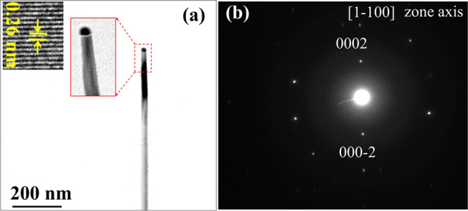
(a) TEM image of GaN NWs grown on GaN substrate using agglomeration conditions of Exp-750_Set(4.14)In and (b) SAED diffraction pattern of the same GaN NW.
The compositional evidence of alloy droplets was confirmed by performing the EDS analysis of droplets before and after the growth of NW. The composition of metals inside the alloy droplet (prior to the growth of NWs) was confirmed by the SEM–EDS because the transfer of droplets to the TEM grid was not possible. However, TEM–EDS was performed for the alloy droplet atop of GaN NW. For the SEM–EDS analysis, the In–Ga–Au alloy droplets (Exp-750_Set-(2.07)In) were selected because they contain all of the incorporated metals. Figure 10a shows the corresponding SEM–EDS spectrum of In–Ga–Au alloy droplets, which reveals the incorporation of In, Ga, and Au metals inside droplets. Figure 10b shows the TEM–EDS line spectrum of top end of single GaN NW grown using agglomeration conditions of Exp-750_Set-(2.07). There are two regions in the line spectrum; the spectrum of catalyst (0–20 nm) shows an excess amount of Au, whereas in the NW region (20–50 nm) near the catalyst, the Ga composition is high. In the selected region, the spectrum of In was not shown, even though it was observed in agglomeration, which confirms that the In is incorporated at the bottom of NWs to form InGaN or InN.
Figure 10.

(a) SEM–EDS spectrum of In–Ga–Au alloy droplets and (b) TEM–EDS line spectrum of catalyst atop of GaN NW.
4. Conclusions
The agglomeration behavior of Ga–Au and In–Ga–Au alloy was investigated on GaN and sapphire substrates at different agglomeration temperatures by varying In and Au composition. For the optimization of growth of NWs, the detailed investigation of agglomeration step is an effective approach. Based on the experimental findings, the best agglomeration temperature for the growth of GaN NWs in all cases is 750 °C for 900 s. Without In composition in Ga–Au alloy catalyst, the lower thickness of Au film (1 and 5 Å) as metal catalyst is recommended. However, for a lower agglomeration temperature such as 650 °C, the In incorporation is necessary for proper agglomeration of Ga–Au alloy droplets, otherwise the alloy droplets exhibit irregular islands, which affects the growth of NWs. Depending on the thickness of Au film and In composition during the agglomeration process, the morphology of the GaN NWs can be tailored. With fixed V/III ratio and reactor pressure, the crystallographic orientation of GaN NWs was tuned from m- to c-axis by increasing the In composition in the In–Ga–Au alloy catalyst. A degradation in the morphology of the GaN NWs was observed with increase in agglomeration temperature up to 850 °C because of the instability in Ga–Au and In–Ga–Au alloy droplets at high temperatures.
By maintaining the agglomeration temperature at 750 °C and by incorporating In with a TMIn flow rate of 2.07 μmol/min, the m-axis NWs with improved morphology were grown on GaN and sapphire substrates. However, by increasing the TMIn flow to 4.14 μmol/min, the NW orientation was tuned from the m-axis to c-axis. With increase in In composition (TMIn flow: 4.14 μmol/min) and agglomeration temperature, NW bushes are observed on the sapphire substrate due to the larger size of In–Ga–Au alloy droplet.
Acknowledgments
This work was supported by the National Research Foundation of Korea (NRF) funded by the Ministry of Education, Science, and Technology (2018R1A6A1A03024334, NRF-2019R1A2C1006360). The samples were grown using MOCVD(Aixtron-CS15276) at Energy Convergence Core Facility in Chonnam National University.
Supporting Information Available
The Supporting Information is available free of charge at https://pubs.acs.org/doi/10.1021/acsomega.0c05587.
SEM images of Au agglomeration and the growth of GaN NWs on GaN and sapphire substrates (PDF)
The authors declare no competing financial interest.
Supplementary Material
References
- Kim H.-M.; Kang T. W.; Chung K. S. Nanoscale Ultraviolet-Light-Emitting Diodes Using Wide-Bandgap Gallium Nitride Nanorods. Adv. Mater. 2003, 15, 567–569. 10.1002/adma.200304554. [DOI] [Google Scholar]
- Lim W.; Wright J. S.; Gila B. P.; Pearton S. J.; Ren F.; Lai W.-T.; Chen L.-C.; Hu M.-S.; Chen K.-H. Selective-Hydrogen Sensing at Room Temperature with Pt-Coated InN Nanobelts. Appl. Phys. Lett. 2008, 93, 202109 10.1063/1.3033548. [DOI] [Google Scholar]
- Waseem A.; Johar M. A.; Hassan M. A.; Bagal I. V.; Ha J.-S.; Lee J. K.; Ryu S.-W. Effect of Crystal Orientation of GaN/V2O5 Core-Shell Nanowires on Piezoelectric Nanogenerators. Nano Energy 2019, 60, 413–423. 10.1016/j.nanoen.2019.03.075. [DOI] [Google Scholar]
- Peng Y.; Que M.; Lee H. E.; Bao R.; Wang X.; Lu J.; Yuan Z.; Li X.; Tao J.; Sun J.; Zhai J.; Lee K. J.; Pan C. Achieving High-Resolution Pressure Mapping via Flexible GaN/ ZnO Nanowire LEDs Array by Piezo-Phototronic Effect. Nano Energy 2019, 58, 633–640. 10.1016/j.nanoen.2019.01.076. [DOI] [Google Scholar]
- Tawfik W. Z.; Lee J. K. Numerical Analysis of the Temperature Impact on Performance of GaN-Based 460-Nm Light-Emitting Diode. J. Nanosci. Nanotechnol. 2018, 18, 1772–1776. 10.1166/jnn.2018.14942. [DOI] [PubMed] [Google Scholar]
- Tawfik W. Z.; Hyun G. Y.; Lee S. J.; Ryu S.-W.; Ha J.-S.; Lee J. K. Enhanced Performance of GaN-Based LEDs via Electroplating of a Patterned Copper Layer on the Backside. J. Mater. Sci. 2018, 53, 8878–8886. 10.1007/s10853-018-2177-8. [DOI] [Google Scholar]
- DenBaars S. P.; Feezell D.; Kelchner K.; Pimputkar S.; Pan C.-C.; Yen C.-C.; Tanaka S.; Zhao Y.; Pfaff N.; Farrell R.; Iza M.; Keller S.; Mishra U.; Speck J. S.; Nakamura S. Development of Gallium-Nitride-Based Light-Emitting Diodes (LEDs) and Laser Diodes for Energy-Efficient Lighting and Displays. Acta Mater. 2013, 61, 945–951. 10.1016/j.actamat.2012.10.042. [DOI] [Google Scholar]
- Waseem A.; Johar M. A.; Hassan M. A.; Bagal I. V.; Ha J.-S.; Lee J. K.; Ryu S.-W. Enhanced Stability of Piezoelectric Nanogenerator Based on GaN/V2O5 Core-Shell Nanowires with Capacitive Contact. Nanotechnology 2019, 31, 075401 10.1088/1361-6528/ab53b8. [DOI] [PubMed] [Google Scholar]
- Waseem A.; Johar M. A.; Hassan M. A.; Bagal I. V.; Ha J.-S.; Lee J. K.; Ryu S.-W. Cu2O Heterostructured GaN Thin Film and GaN Nanowire Piezoelectric Nanogenerators. Phys. Status Solidi A 2020, 217, 1900798 10.1002/pssa.201900798. [DOI] [Google Scholar]
- Johar M.; Hassan M.; Waseem A.; Ha J.-S.; Lee J.; Ryu S.-W. Stable and High Piezoelectric Output of GaN Nanowire-Based Lead-Free Piezoelectric Nanogenerator by Suppression of Internal Screening. Nanomaterials 2018, 8, 437 10.3390/nano8060437. [DOI] [PMC free article] [PubMed] [Google Scholar]
- Zeng S. W.; Zhang B. P.; Sun J. W.; Cai J. F.; Chen C.; Yu J. Z. Substantial Photo-Response of InGaN p–i–n Homojunction Solar Cells. Semicond. Sci. Technol. 2009, 24, 055009 10.1088/0268-1242/24/5/055009. [DOI] [Google Scholar]
- Ertekin E.; Greaney P. A.; Chrzan D. C.; Sands T. D. Equilibrium Limits of Coherency in Strained Nanowire Heterostructures. J. Appl. Phys. 2005, 97, 114325 10.1063/1.1903106. [DOI] [Google Scholar]
- Miyamoto Y.; Hirata M. Growth of New Form Germanium Whiskers. Jpn. J. Appl. Phys. 1975, 14, 1419 10.1143/JJAP.14.1419. [DOI] [Google Scholar]
- Trentler T. J.; Hickman K. M.; Goel S. C.; Viano A. M.; Gibbons P. C.; Buhro W. E. Solution-Liquid-Solid Growth of Crystalline III-V Semiconductors: An Analogy to Vapor-Liquid-Solid Growth. Science 1995, 270, 1791–1794. 10.1126/science.270.5243.1791. [DOI] [Google Scholar]
- Yang S.; Ge C.; Liu Z.; Fang Y.; Li Z.; Kuang D.; Su C. Novel Ga-Doped, Self-Supported, Independent Aligned ZnO Nanorods: One-Pot Hydrothermal Synthesis and Structurally Enhanced Photocatalytic Performance. RSC Adv. 2011, 1, 1691–1694. 10.1039/c1ra00555c. [DOI] [Google Scholar]
- Davidson F. M.; Lee D. C.; Fanfair D. D.; Korgel B. A. Lamellar Twinning in Semiconductor Nanowires. J. Phys. Chem. C 2007, 111, 2929–2935. 10.1021/jp0672205. [DOI] [Google Scholar]
- Bootsma G. A.; Gassen H. J. A Quantitative Study on the Growth of Silicon Whiskers from Silane and Germanium Whiskers from Germane. J. Cryst. Growth 1971, 10, 223–234. 10.1016/0022-0248(71)90188-6. [DOI] [Google Scholar]
- Wagner R. S.; Ellis W. C. Vapor-liquid-solid mechanism of single crystal Growth. Appl. Phys. Lett. 1964, 4, 89–90. 10.1063/1.1753975. [DOI] [Google Scholar]
- Zhang C.; Miao X.; Chabak K. D.; Li X. A Review of III–V Planar Nanowire Arrays: Selective Lateral VLS Epitaxy and 3D Transistors. J. Phys. Appl. Phys. 2017, 50, 393001 10.1088/1361-6463/aa7e42. [DOI] [Google Scholar]
- Redwing J. M.; Miao X.; Li X.. Vapor–Liquid–Solid Growth of Semiconductor Nanowires. In Handbook of Crystal Growth: Thin Films and Epitaxy, 2nd ed.; Elsevier: North-Holland, 2014; pp 399–439. [Google Scholar]
- Nebol’sin V. A.; Shchetinin A. A. Role of Surface Energy in the Vapor–Liquid–Solid Growth of Silicon. Inorg. Mater. 2003, 39, 899–903. 10.1023/A:1025588601262. [DOI] [Google Scholar]
- Duan X.; Lieber C. M. Laser-Assisted Catalytic Growth of Single Crystal GaN Nanowires. J. Am. Chem. Soc. 2000, 122, 188–189. 10.1021/ja993713u. [DOI] [Google Scholar]
- Lekhal K.; Avit G.; André Y.; Trassoudaine A.; Gil E.; Varenne C.; Bougerol C.; Monier G.; Castelluci D. Catalyst-Assisted Hydride Vapor Phase Epitaxy of GaN Nanowires: Exceptional Length and Constant Rod-like Shape Capability. Nanotechnology 2012, 23, 405601 10.1088/0957-4484/23/40/405601. [DOI] [PubMed] [Google Scholar]
- Madapu K. K.; Dhara S.; Amirthapandian S.; Pandian R. Indium Assisted Growth of GaN Nanowires at Low Temperatures. AIP Conf. Proc. 2013, 1512, 278–279. [Google Scholar]
- Oh E.; Lee B. W.; Shim S.; Lee K.-Y.; Oh H.; Choi H.-J.; Son B. H.; Ahn Y. H.; Dang L. S. Platinum Assisted Vapor-Liquid-Solid Growth of GaN Nanowires and Their Properties. J. Korean Phys. Soc. 2010, 56, 100–103. 10.3938/jkps.56.100. [DOI] [Google Scholar]
- Zhang J.; Zhang L. Growth of Semiconductor Gallium Nitride Nanowires with Different Catalysts. J. Vac. Sci. Technol., B: Microelectron. Nanometer Struct. 2003, 21, 2415. 10.1116/1.1625968. [DOI] [Google Scholar]
- Wu S.; Wang L.; Yi X.; Liu Z.; Yan J.; Yuan G.; Wei T.; Wang J.; Li J. Crystallographic Orientation Control and Optical Properties of GaN Nanowires. RSC Adv. 2018, 8, 2181–2187. 10.1039/C7RA11408G. [DOI] [PMC free article] [PubMed] [Google Scholar]
- Liu Y.; Peng Y.; Guo J.; La D.; Xu Z. The Effect of V/III Ratio on the Morphology and Structure of GaAs Nanowires by MOCVD. AIP Adv. 2018, 8, 055108 10.1063/1.5028350. [DOI] [Google Scholar]
- Kuykendall T. R.; Altoe M. V. P.; Ogletree D. F.; Aloni S. Catalyst-Directed Crystallographic Orientation Control of GaN Nanowire Growth. Nano Lett. 2014, 14, 6767–6773. 10.1021/nl502079v. [DOI] [PubMed] [Google Scholar]
- Wang J.; Plissard S. R.; Verheijen M. A.; Feiner L.-F.; Cavalli A.; Bakkers E. P. A. M. Reversible Switching of InP Nanowire Growth Direction by Catalyst Engineering. Nano Lett. 2013, 13, 3802–3806. 10.1021/nl401767b. [DOI] [PubMed] [Google Scholar]
- Joyce H. J.; Wong-Leung J.; Gao Q.; Tan H. H.; Jagadish C. Phase Perfection in Zinc Blende and Wurtzite III–V Nanowires Using Basic Growth Parameters. Nano Lett. 2010, 10, 908–915. 10.1021/nl903688v. [DOI] [PubMed] [Google Scholar]
- Hofmann S.; Sharma R.; Wirth C. T.; Cervantes-Sodi F.; Ducati C.; Kasama T.; Dunin-Borkowski R. E.; Drucker J.; Bennett P.; Robertson J. Ledge-Flow-Controlled Catalyst Interface Dynamics during Si Nanowire Growth. Nat. Mater. 2008, 7, 372–375. 10.1038/nmat2140. [DOI] [PubMed] [Google Scholar]
- Wacaser B. A.; Dick K. A.; Johansson J.; Borgström M. T.; Deppert K.; Samuelson L. Preferential Interface Nucleation: An Expansion of the VLS Growth Mechanism for Nanowires. Adv. Mater. 2009, 21, 153–165. 10.1002/adma.200800440. [DOI] [Google Scholar]
- Glas F.; Harmand J.-C.; Patriarche G. Why Does Wurtzite Form in Nanowires of III-V Zinc Blende Semiconductors?. Phys. Rev. Lett. 2007, 99, 146101 10.1103/PhysRevLett.99.146101. [DOI] [PubMed] [Google Scholar]
- Kuo C.-K.; Hsu C.-W.; Wu C.-T.; Lan Z.-H.; Mou C.-Y.; Chen C.-C.; Yang Y.-J.; Chen L.-C.; Chen K.-H. Self-Regulating and Diameter-Selective Growth of GaN Nanowires. Nanotechnology 2006, 17, S332–S337. 10.1088/0957-4484/17/11/S17. [DOI] [Google Scholar]
- Elliott R. P.; Shunk F. A. The Au–Ga (Gold-Gallium) System. Bull. Alloy Phase Diagrams 1981, 2, 356–358. 10.1007/BF02868293. [DOI] [Google Scholar]
- Ghasemi M.; Sundman B.; Fries S. G.; Johansson J. The Thermodynamic Assessment of the Au–In–Ga System. J. Alloys Compd. 2014, 600, 178–185. 10.1016/j.jallcom.2014.02.071. [DOI] [Google Scholar]
- Koleske D. D.; Wickenden A. E.; Henry R. L.; Culbertson J. C.; Twigg M. E. GaN Decomposition in H2 and N2 at MOVPE Temperatures and Pressures. J. Cryst. Growth 2001, 223, 466–483. 10.1016/S0022-0248(01)00617-0. [DOI] [Google Scholar]
- Stringfellow G. B.Organometallic Vapor-Phase Epitaxy; Elsevier, 1999. [Google Scholar]
Associated Data
This section collects any data citations, data availability statements, or supplementary materials included in this article.