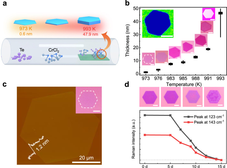
Fig. 1. Synthesis and characterization of 1T-CrTe2 single crystals on SiO2/Si substrates.
a Schematic of the grown 1T-CrTe2 single crystals by the CVD method. CrCl2 and Te powders are used as Cr and Te sources, respectively, to realize the reaction at a relatively low temperature. b The sample thickness as a function of growth temperature with the corresponding OM images. The black line and the black rectangle indicate the range of the thickness and the averaged thickness of the samples grown at a given temperature, respectively. The top-left inset shows the Raman mapping image of 1T-CrTe2 based on the vibration mode at 123.6 cm-1. The thickness of the sample is about 10.0 nm. c AFM image and the corresponding OM image (upper right inset) of a typical 1T-CrTe2 hexagonal nanoflake on a 285 nm SiO2/Si substrate. The height profile in the lower left inset shows that this sample flake is ~1.2 nm thick. d Environmental stability investigation based on a ~4-nm thick sample. Upper panels are OM images of 1T-CrTe2 samples that are exposed in the ambient environment for 0, 5, 10, and 15 days, respectively. Below is the evolution of Raman intensity with time progression. The gray dotted line indicates the zero Raman signal. Scale bars in b, c, and d: 20 μm.

