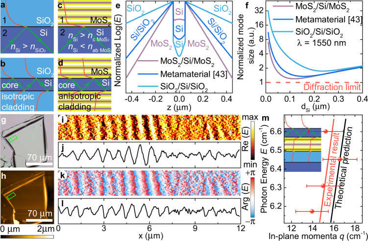
Fig. 5. Transparent sub-diffraction optics.
a Traditional total internal reflection with two isotropic media: above the critical angle, the light is reflected from the interface giving a decaying wave for a lower refractive index medium. b The decaying wave penetrates low refractive index material resulting in strong cross-talk between neighboring waveguides and limits the current on-chip photonics. c Relaxed total internal reflection: the out-of-plane dielectric refractive index is less than that of isotropic material, while the high in-plane refractive index provides fast decay of electric field amplitude in the first medium. d Anisotropic material gives rise to a planar waveguide with strong light confinement. The red curves for the a–d schematically show electric field amplitude. e Comparison of electric field distributions for MoS2/Si/MoS2, metamaterial(SiO2/Si)/Si/metamaterial(SiO2/Si)43 systems reveals that giant anisotropy causes giant light compression. f Light confinement in MoS2/Si/MoS2 allows for tackling the diffraction limit compared with traditionally used SiO2/Si/SiO2 and recently introduced43 metamaterial cladding with alternating layers of Si and SiO2 with silicon as a core. Mode size is normalized to the diffraction limit defined as λ/(2∙ncore). g, h Optical and AFM topography images of the flake with 190 nm covered silicon. i–l Near field images, real part Re (E) and phase Arg (E), with the corresponding line scans of the electric field taken at λ = 1550 nm from the area of g–h indicated by a green rectangular. (s-SNOM images taken at different wavelengths are collected in Supplementary Note 5). m Comparison between theoretical and experimental mode dispersion. The error bars show the uncertainty in the determination of mode in-plane momenta q from near-field images displayed in i–l. The inset is an artistic representation of the investigated system Air/Si (195 nm)/MoS2 (285 nm)/SiO2 (285 nm)/Si.

