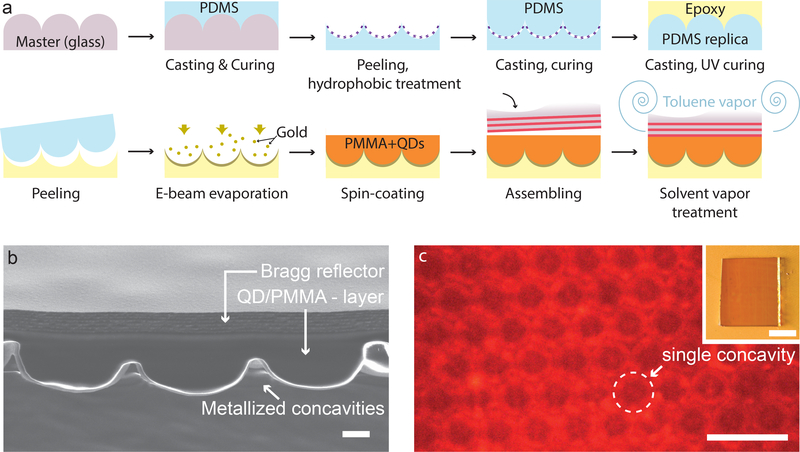
Figure 2: The fabricated SLED surface.
a) Schematic of the manufacturing procedure. The patterned epoxy substrate was obtained by a three-step replica moulding procedure, consisting in casting PDMS on a glass master, PDMS casting on PDMS, and epoxy casting on the PDMS replica. Then, the SLED surface was assembled by adding the metal reflector, QDs and Bragg reflector on top of the patterned epoxy. b) Cross-sectional SEM view of the SLED device showing the patterned bottom surface, the QD-doped PMMA layer and the Bragg reflector; scale bar: 1μm. c) Top view of the complete device obtained by fluorescence microscopy with the microscope’s focus plane on the bottom reflector; scale bar: 10μm. Inset shows a macroscopic top-view of the assembled SLED surface; scale bar: 1mm.

