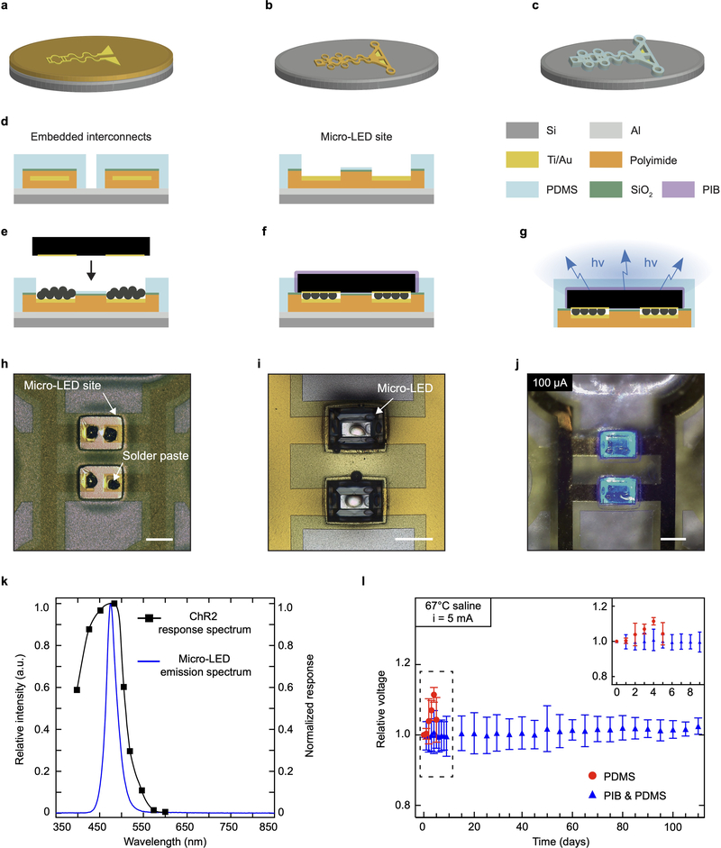
Extended Data Fig. 4: Microfabrication of the flexible micro-LED array to target activation of ChR2 in vivo.
a – c, Schematic illustration of the microfabrication process. Patterning of a Ti/Au film on a polyimide substrate (a). Polyimide superstrate covering of the film followed by patterning of the polyimide stack (b). Encapsulation in PDMS and subsequent patterning of the silicone layer (c). d, Schematic cross-sections of the interconnects and micro-LED site of integration. e – g, Illustrations of the micro-LED integration process. Printing of soldering paste on the interconnect pads followed by precise placement of the micro-LED (e). The reflow of the paste ensures mechanical and electrical interfacing. Printing of polyisobuthylene (PIB) on the micro-LED surface (f). PDMS encapsulation and release from the silicon carrier (g). h – j, Representative optical micrographs, such as solder paste printing (h), micro-LED deposition (i) and activation (j). Scale bar: 250 μm. k, Relative intensity associated with micro-LED emission spectrum, or spectral flux, and ChR2 normalized response spectrum. l, Relative changes in voltage for devices placed in 67 °C saline depending on micro-LED encapsulation material. Arrays only encapsulated with PDMS fail after day 7. n = 3 devices per group; mean ± s.d.

