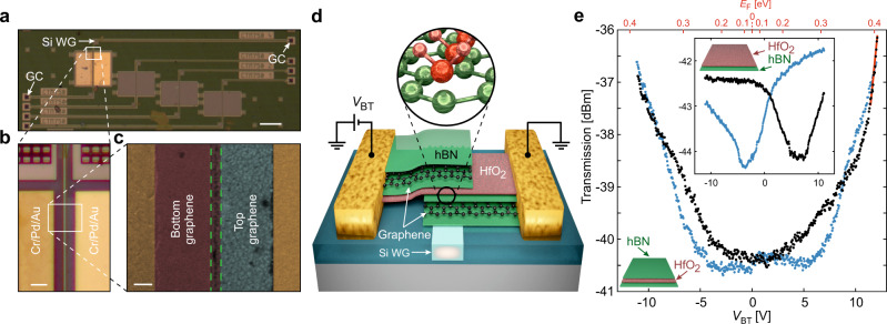
Fig. 1. Device geometry and static characterization.
a Optical image of a photonic device consisting of two grating couplers (GC), a silicon optical waveguide (Si WG), and an hBN–HfO2–hBN-based graphene EA modulator on top (see zoom-in optical (panel b) and scanning electron microscope (SEM) (panel c) images for details). In panel c, the metal contacts are yellow/brown and the bottom and top graphene electrodes violet and light blue, respectively. The core of the waveguide is highlighted by the green dashed lines. The white scale bars in panel a, b, and c are 100, 5, and 1 μm, respectively. d Electrical connections and schematic cross-section of an EA modulator with an hBN–HfO2–hBN dielectric. The top and bottom graphene electrodes are fully encapsulated by hBN (in green) protecting both graphene electrodes from the out-of-plane dangling bonds typical of 3D oxide materials, e.g., HfO2 (in red). See inset for a molecular representation. e Transmission curves as a function of the voltage between the bottom and top graphene electrodes (VBT axis, bottom) and the Fermi energy at the graphene electrodes (EF axis, top) for the EA modulator in panel a with an hBN–HfO2–hBN dielectric (see sketch). The 1550 nm excitation power was set to 0 dBm. The forward and backward voltage sweeps (black and blue, respectively) show no major hysteresis compared to a modulator with an hBN–HfO2 dielectric (see inset). The red line is a linear fit to the forward voltage sweep within a 0.5 V voltage span (extracted slope: 2.2 dBV−1).

