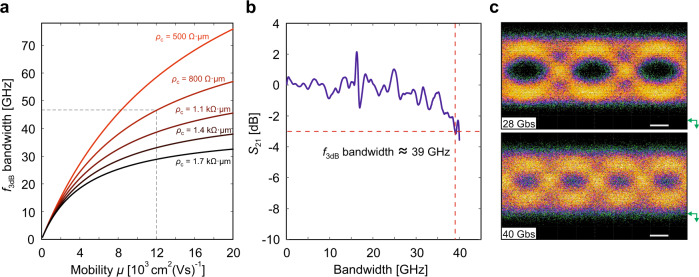
Fig. 2. Dynamic characterization.
a f3dB bandwidth as a function of the charge carrier-dependent mobility (μ) and the contact resistivity (ρc) calculated for a device with the same geometry and dielectric combination as the device in Fig. 1 (see Supplementary Note 11). The dashed lines indicate the expected f3dB ~46 GHz at μ ~12,000 cm2 V−1 s−1 (evaluated at VBT = 10.4 V, refer to panel b). b Measured electro-optical S21 frequency response of the EA modulator at VBT = 10.4 V and VAC = 200 mV, without de-embedding, i.e., including the contributions of the setup and photodetector (see Supplementary Note 12). c In all, 231 − 1 pseudo-random binary sequence non-return-to-zero eye diagram at 28 and 40 Gbps. The EA modulator is d.c. biased at VBT = 11 V and driven by a VAC = 3.5 V peak-to-peak RF signal. The eye diagram measured at 40 Gbps has a 5.2 dB ER and a 2.28 dB signal-to-noise ratio (SNR). The green arrows indicate the 0 W baseline, and the white scale bar corresponds to 10 ps.

