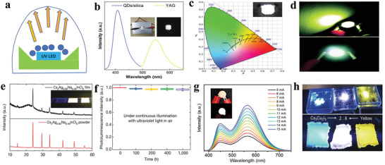
Figure 11.

a) Schematic of phosphor‐converted LED. b) EL spectrum of the WLED by integrating blue‐emitting Cs3Bi2Br9 NCs and yellow‐emitting rare‐earth phosphor Y3Al5O12. Inset: device photos of NCs/silica composites combined with Y3Al5O12 (off and on). Reproduced with permission.[ 58 ] Copyright 2017, Wiley‐VCH. c) CIE color coordinates of WLED device combined by Cs2SnCl6:2.75%Bi3+/Ba2Sr2SiO4:Eu2+/GaAlSiN3:Eu2+/365 chip and inset image of operating LED. Reproduced with permission.[ 16e ] Copyright 2018, Wiley‐VCH. d) 365 nm UV pumped single yellow‐emitting (OCTAm)2SnBr4 LED and WLED fabricated by (OCTAm)SnBr4/BaMgAl10O17:Eu2+/G2762/365 nm UV chip. Reproduced with permission.[ 56 ] Copyright 2019, Royal Society of Chemistry. e) XRD patterns of a Cs2Ag0.6Na0.4InCl6 films (top) and powder (bottom). The inset displays a 300 nm thick quartz substrate and 500 nm thick Cs2Ag0.6Na0.4InCl6 films under the excitation of 254 nm. f) Operational stability of Cs2Ag0.6Na0.4InCl6 devices, measured in air without any encapsulation. Reproduced with permission.[ 60 ] Copyright 2018, Springer Nature. g) EL spectra of a WLED at different driving currents, the insets show the device when off and on. Reproduced with permission.[ 132 ] Copyright 2018, Royal Society of Chemistry. h) Photograph of Cs3Cu2I5, a yellow phosphor, and its mixtures (from left to right: Cs3Cu2I5, mixture of 2:8, yellow phosphor) under UV excitation (top) and films prepared by kneading the powders into polydimethylsiloxane matrix (bottom). Reproduced with permission.[ 61 ] Copyright 2018, Wiley‐VCH.
