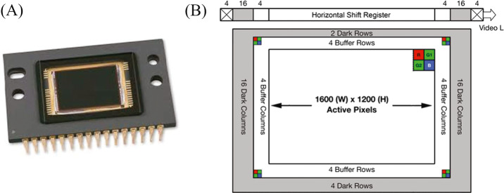
Fig. 3.
(A) Vendor image of the ON Semi KAI-2020 detector; (B) Simplified schematic of the Kodak KAI-2020 interline transfer CCD. Each pixel is overlain by a Bayer pattern filter, shown as the colored cells, bonded directly to the CCD’s active pixels. In this view, pixel clocking is up and to the right (first pixel read out is G1). The active region consists of pixels surrounded by buffer pixels, dark shielded pixels, and the horizontal shift register. Note that the Bayer pattern pixels are not shown to scale in the image. Note that the schematic is drawn looking down on the detector. Images are displayed from the perspective of the detector looking out. Therefore, while the readout and pixel is in the upper-right of this schematic, they are instead in the upper left of the camera images displayed throughout this manuscript. Images are adapted from the online vendor manual (https://www.onsemi.com/pub/Collateral/KAI-2020-D.eps)

