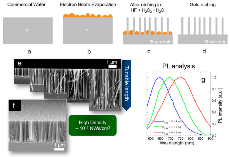
Figure 8.
Scheme of Si NW synthesis by thin film MACE: (a) native oxide etching, (b) thin metal film deposition by EBE, (c) metal-assisted chemical etching, (d) gold etching. All the processes are performed at room temperature. (e) Cross-section SEM images showing the possibility to tune the NW lengths from hundreds of nanometers to several micrometers. (f) Tilted Cross-section SEM showing the high NW density of about 1012 NWs/cm2. Raman analysis of the first order stokes silicon peak. The average Si NW diameter is obtained for each different metal by fitting the Raman peak with the Campbell-Fauchet model [134]. (g) Normalized PL spectra of the different NW samples.

