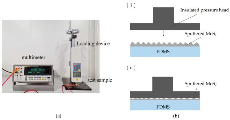
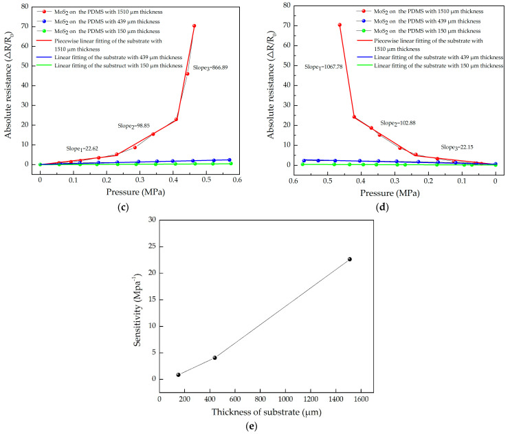
Figure 10.
The piezoresistive property test of sputtered MoS2 film: (a) the piezoresistive testing system for thin films; (b) the schematic diagram of the film surface compression: (i) the state of Scheme 2 before pressure; (ii) the state of sputtered MoS2 under pressure; (c,d) pressure test curves of MoS2 films deposited on PDMS substrates with different thicknesses at the power of 350 W; (e) the relationship diagram between the thickness of the substrate and the sensitivity of MoS2 sputtered on the substrate at 0–0.23 MPa.


