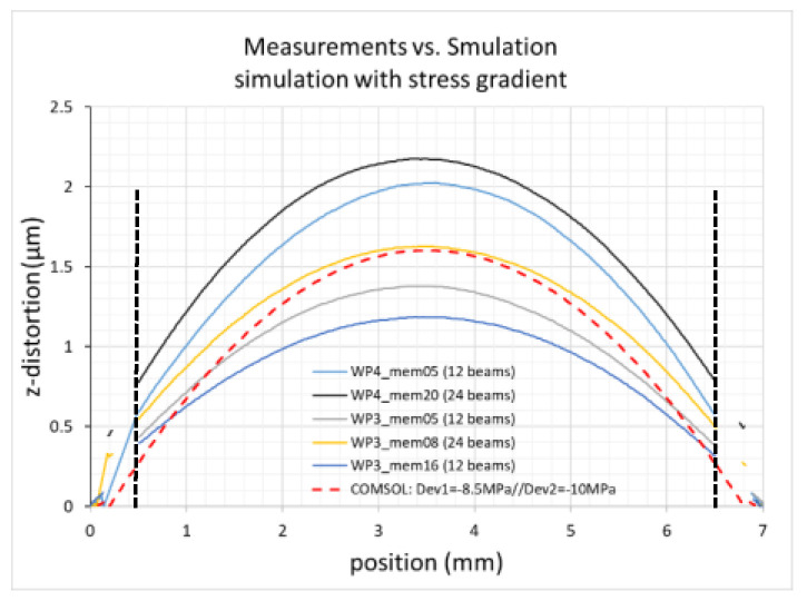
Figure 9.
Evaluation of membrane distortion at U = 0 V. Shown are experimental results from 5 different devices made from 2 different wafers (mem05 and mem16: 12 tangential beams, mem08 and mem20: 24 tangential beams). As a comparison, a COMSOL simulation (red) for a model with 24 beams is shown where the device layer was split into two layers with different compressive stress values: a 9 µm thick layer with a residual stress of −10MPa and a 1 µm thick layer with −8.5 MPa; the dotted vertical lines mark the positions of the outer membrane rim.

