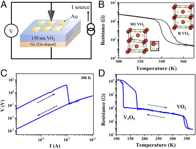
Fig. 1.
Nonvolatile resistive switching in Au/VO2/Ge vertical devices. (A) Schematic illustration of the out-of-plane VO2 device and the measurement setup. The Au and highly doped Ge are top and bottom electrodes, respectively. (B) Resistance as a function of temperature of 150-nm VO2 film. (Inset) Low-temperature insulating VO2 monoclinic phase (M1 VO2) and high-temperature metallic VO2 rutile phase (R VO2). (C) Room-temperature I-V curve. (D) After electroforming, the R-T curve of the VO2 device shows another metal-insulator transition behavior at low temperatures.

