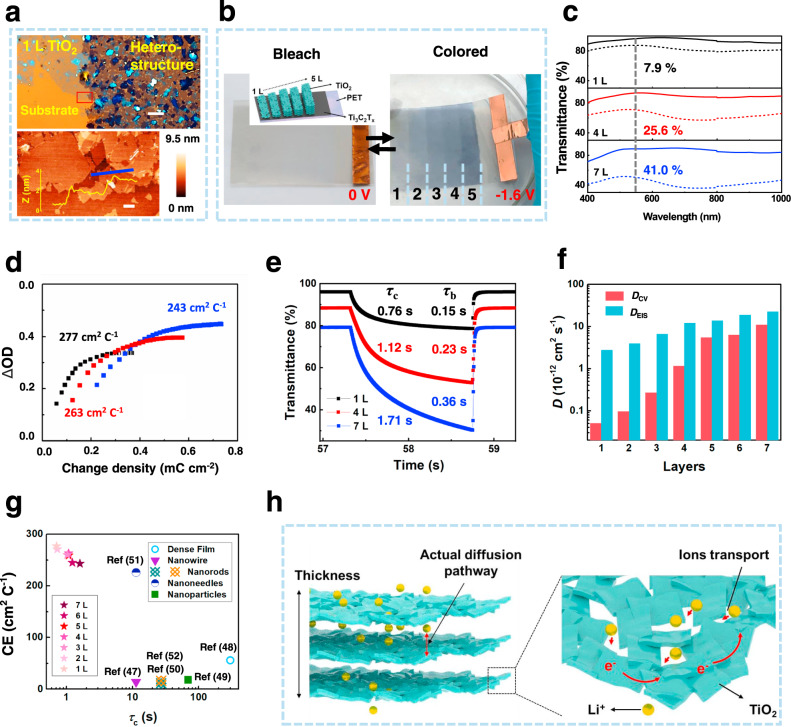
Fig. 4. Electrochromic properties of the TiO2/Ti3C2Tx heterostructure.
a OM image of a junction between a 1-layer TiO2 film and the TiO2/Ti3C2Tx heterostructure (Top) (Scale bar: 10 μm), and AFM image and the height profile of across the junction in corresponding area marked in the OM image (Bottom) (Scale bar: 1 μm); b Photographs of the TiO2/Ti3C2Tx/PET film with different layers of TiO2 at the bleaching state (no bias) and the colored state (biased at −1.6 V). Inset: structure of TiO2/Ti3C2Tx/PET film with different TiO2 layers; c Optical transmittance spectra with 1, 4, and 7 layers of TiO2 at the biases of 0 V (solid) and −1.6 V (dotted); d Optical density change (ΔOD) as a function of the injected charge density for the heterostructures with 1, 4, and 7 layers of TiO2; e Temporal response of the transmittance at 550 nm of the heterostructures with 1, 4, and 7 layers of TiO2; f Diffusion coefficients (D) of the heterostructures with 1−7 layers of TiO2 extracted from the EIS and CV measurements; g Coloration efficiency (CE) as a function of coloration time (τc) for the TiO2/Ti3C2Tx heterostructures and previously reported TiO2-based structures; h Schematic of the pathways of electron conduction and ion diffusion within the self-assembled TiO2 thin film.

