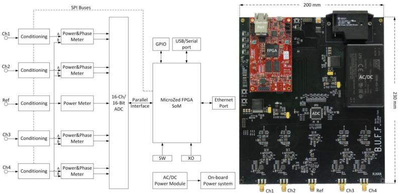
Figure 1.
Left: System block diagram of the supervision module. One power meter was implemented in the reference channel whereas identical power and phase meters were implemented in the radio frequency (RF) input channels. Two serial peripheral interface (SPI) buses were routed from the FPGA (field-programmable gate array) to the conditioning chips for configuration. The FPGA receives data from the analog-to-digital converter chip through its parallel interface. The Ethernet interface was utilized for data exchange. The on-board power system distributes various DC (direct current) power supplies to components on the board. GPIO: general-purpose input/output; SoM: system-on-module; SW: switches; XO: crystal oscillator; ADC: analog-to-digital converter. Right: A photo of the supervision module. The red module is a system-on-module unit (AES-Z7MB-7Z020-SOM-I-G, Avnet, Phoenix, AZ, USA). Please note that the photo is rotated by 90 degrees versus the block diagram shown on the left-hand side.

