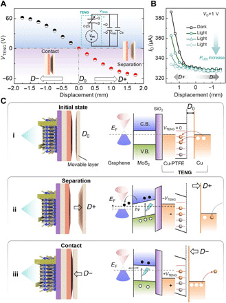
Fig. 2. Mechano-optoelectronic transistor based on Gr/MoS2 heterostructure and corresponding working mechanism.

(A) The TENG output voltage (VTENG) versus displacement (D). Inset: Equivalent circuit diagram for VTENG characterization. (B) Transfer curves (ID versus D) in the dark and under different green light power intensity (PLED). (C) Working mechanism of the mechano-optoelectronic transistor based on Gr/MoS2 heterostructure. Schematic illustrations of the working principles and the corresponding energy band diagram at (i) initial flat-band state, (ii) separation state (D+), and (iii) contact state (D−).
