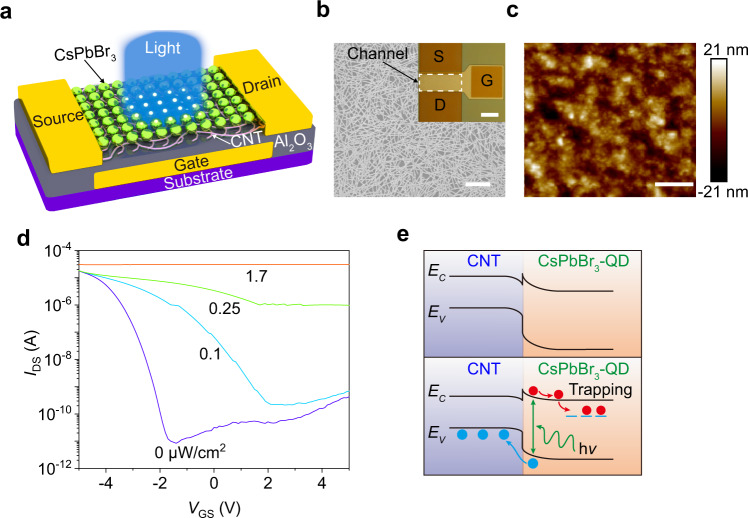
Fig. 1. Device design and characterization.
a Schematic of the phototransistor with a CNT/CsPbBr3-QD channel. b Scanning electron microscope (SEM) image of a CNT film (scale bar, 1 μm). Inset: optical microscope image of the fabricated device (scale bar, 50 μm). c Atomic force microscope (AFM) image of a CsPbBr3-QD film (scale bar, 250 nm). d Room temperature transfer characteristics (IDS – VGS) of the device at VDS = 1 V using a collimated incident beam of laser light with a wavelength λ of 516 nm and power densities (P) increasing from 0 to 1.7 μW/cm2. e Energy band diagram at the light-off (top panel) and light-on states (bottom panel).

