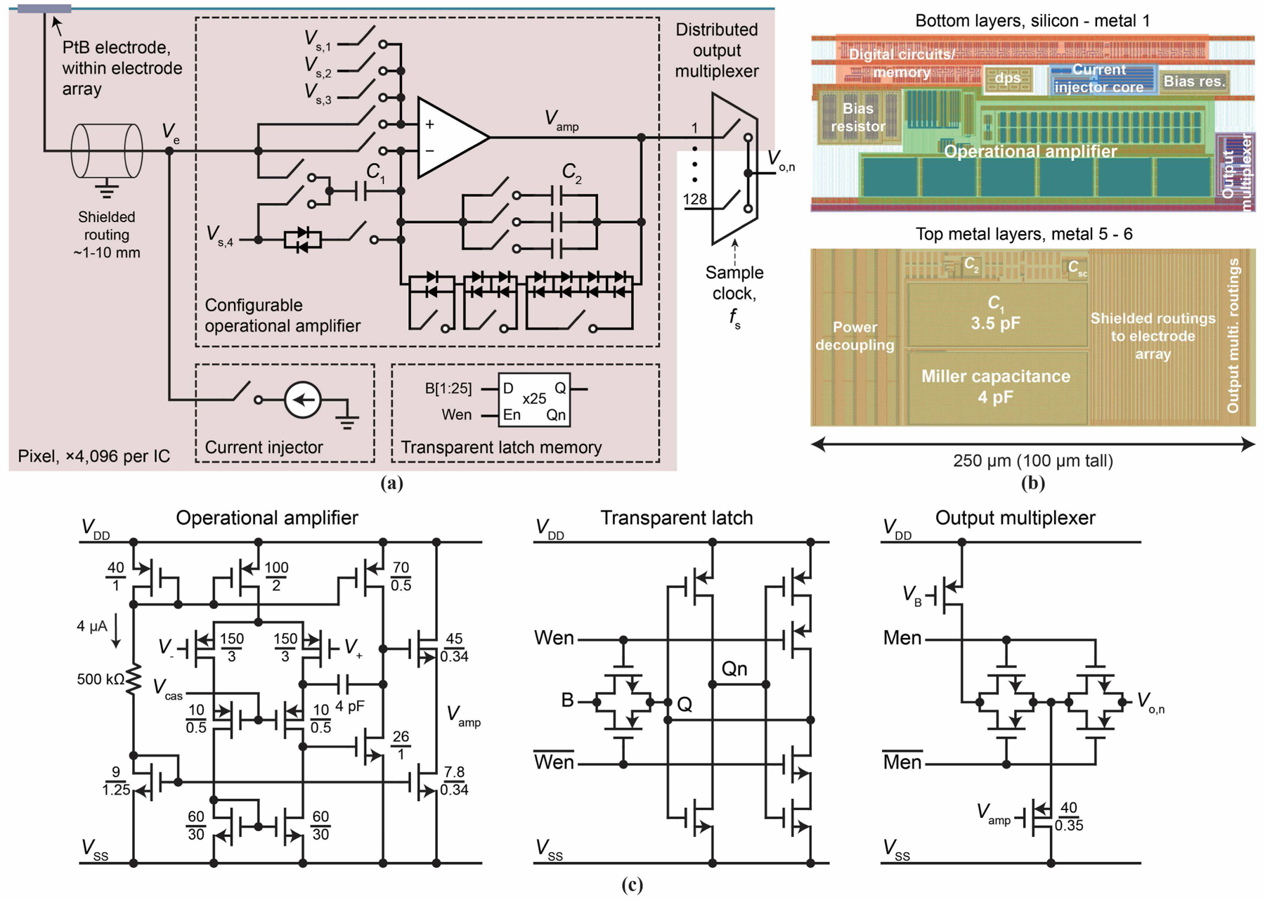
Fig. 3.

(a) Active pixel circuit schematic. The switches (transmission gates) are controlled by the transparent latch memory to configure the pixel for experiments. C1 = 3.5 pF; C2 has the options of adding any of ∼5 fF, ∼20 fF, and ∼100 fF. (b) Active pixel circuit layout. Metal-insulator-metal capacitors are identified on the topmost metal layers. (c) Transistor-level schematics of various pixel components, in particular, op-amp (left), transparent latch (middle), and output multiplexer (right); the schematic of the current injector is shown in detail in Fig. 7.
