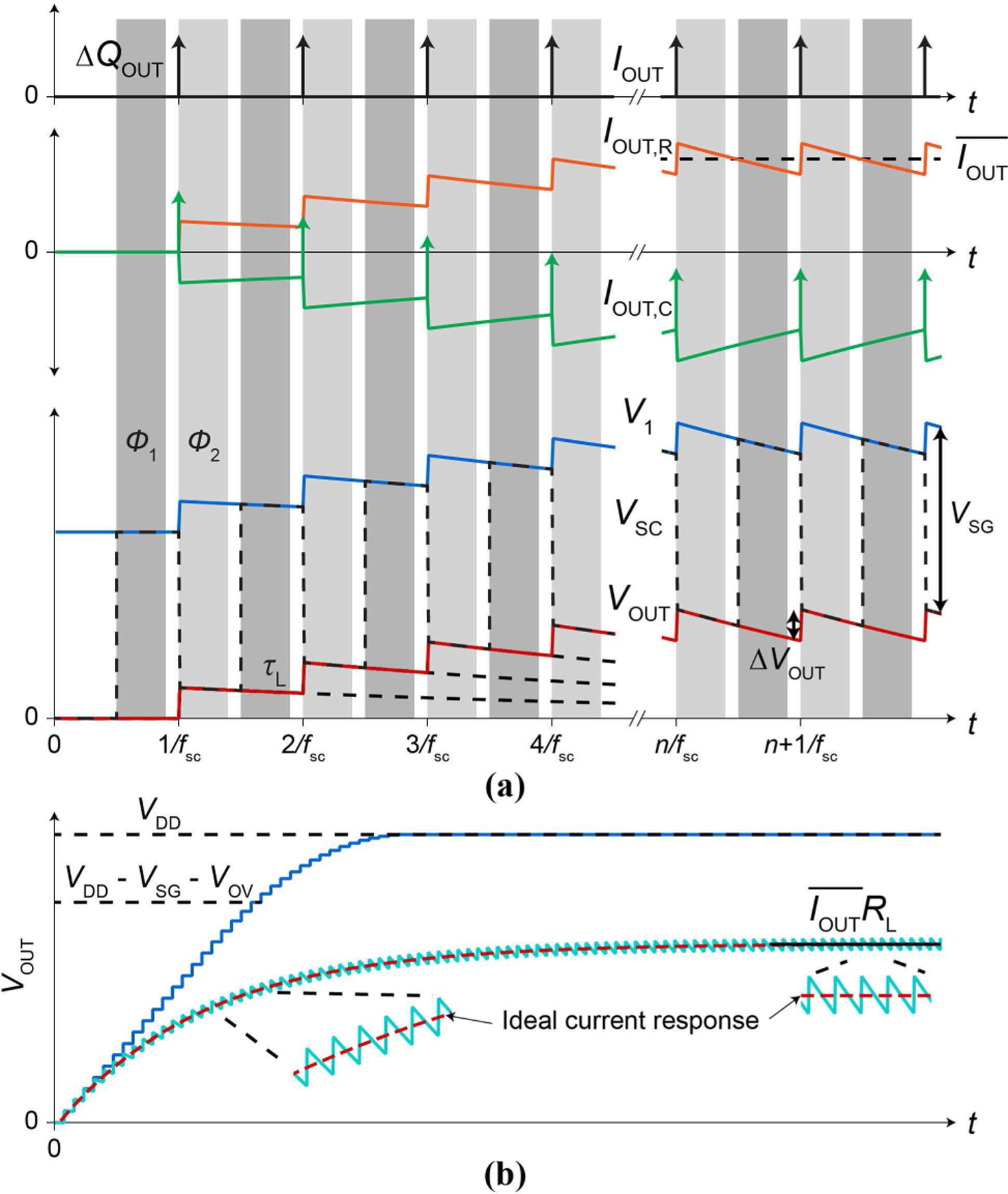
Fig. 6.

(a) Timing diagram for IOUT, IOUT,R IOUT,C, and V1, VSC, VOUT. (b) VOUT(t) for the RLCL load (cyan, solid) in juxtaposition with VOUT(t) for a CL-only load (blue, solid). The response of the RLCL load to an ideal step current is overlaid (red, dashed) for comparison.
