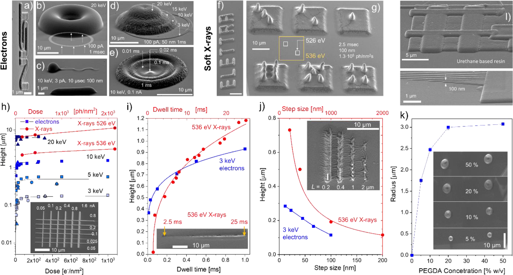
Figure 3.

SEM images of 3D features example patterned using focused electron beam a) – e) and soft X-rays f), g). The numbers inside indicate energy, beam currents (photons intensities), dwell times and step sizes used. a) NIST logo is written with 3 keV electrons (100 pA, 1ms dwell time) using 10 nm pixel size. b) Donut-like gel feature made by writing 1 μm wide ring with a radius of 10 μm. c) Single line flagella-like structure, where the head blob is due to beam parking (elevated dwell time). d) Dome structures formed out of four overlapping coaxial rings by varying electron beam energy and dose e) for every ring. f) ELETTRA logo printed with 536 eV 150 nm wide X-ray beam with 25 ms dwell time. Photon flux ca 2·107 ph/nm2 s and 100 nm step size. g) Dices printed with two photon energies: 13 µm base squares- 536 eV (yellow color coding) and small 2.5 µm squares 526 eV (white color coding), h)-j) SEM measured heights of the dry rectangular and linear gel features as a function of exposure dose h), dwell time i) and step size j) for different energies of electrons (blue) and X-rays (red) beams. The insets show SEM image of gel structure written with variable beam current h), dwell time along its length using 536 eV X-rays i), and step-size L using 536 eV X-rays and 3 keV electrons. k) Size dependence of the grown features on the PEGDA concentration (exposure parameters: 15 keV, 40 pA, 3 s dwell time). l) In-liquid e-beam induced crosslinking of urethane-based resin. Bottom panel demonstrates the writing of very thin (ca. 100 nm wide/tall) lines. Exposure conditions were: 3 keV, 2 pA, 30 s dwell time.
