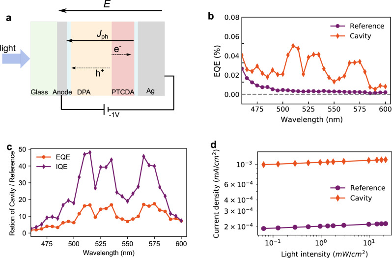
Fig. 4. Photoresponse of the cavity and reference devices.
a The device structures. The anode for the cavity device is 20 nm Ag and 110 nm ITO for the reference device. Spacer layers of mCP and TmPyPB were 5 and 10 nm, respectively. b The EQE of the photodiode under −1 V bias at short circuit condition. c The ratio of EQE and IQE of the cavity and reference devices. d The log–log plot of light intensity (475 nm) dependent photocurrent in cavity and reference devices.

