
Fig. 1.
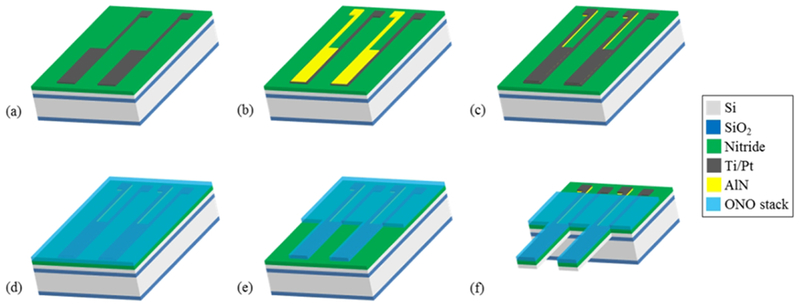
Fabrication of piezoelectric cantilevers. (a) Ti/Pt bottom electrodes and contact pads were deposited on an SOI wafer with insulation layers on the front and backside and patterned via liftoff. (b) Piezoelectric AlN was reactively sputtered and patterned via liftoff. (c) Top metal electrodes and contact pads were deposited and patterned via liftoff. (d) Top insulation layer (ONO) was deposited via PECVD. (e) The insulation layer was patterned by RIE. (f) The front and backside were etched via DRIE to define and release the cantilevers, followed by an HF dip to remove the buried oxide layer.