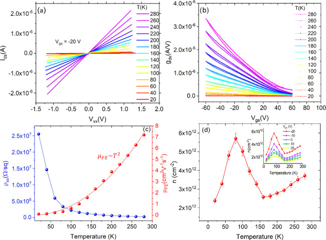
Figure 3.
(a) Ids versus Vxx curves at different temperatures. (b) Transfer characteristics recorded for a loop of the voltage bias at different temperatures. (c) Channel resistivity (blue dots) and field-effect mobility (red dots) as a function of temperature. The superposed red line is the quadratic fit. (d) Carrier density n versus temperature at VGS = −20 V. The inset shows n as a function of temperature at several gate biases. The uncertainties are obtained from the standard error propagation.

