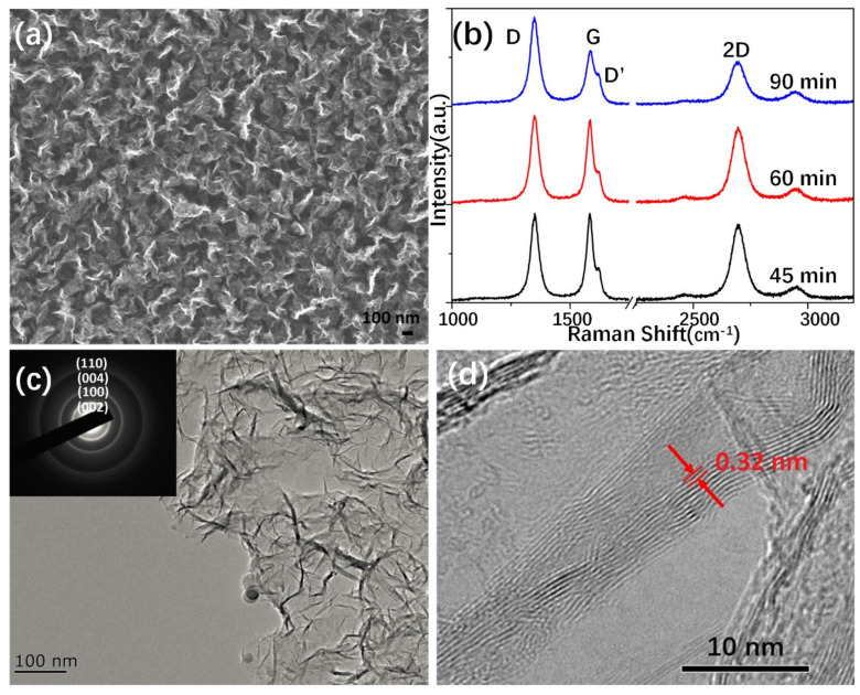
Figure 1.
Characteristics of graphene nanowalls. (a) SEM image of the wrinkled graphene nanowalls grown on silicon. (b) Raman shift of the graphene grown in different time, laser: 532 nm. (c) TEM image and (d) HRTEM image of graphene. The inset in (c) is the selected area electron diffraction (SAED) pattern of the graphene nanosheets.

