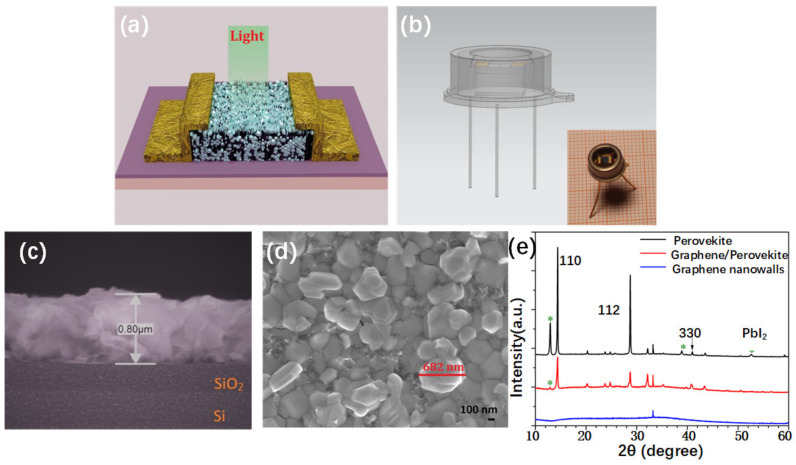
Figure 2.
Schematic diagram of the device and characteristics of the graphene/perovskite hybrid photodetector. (a,b) Configuration of the lateral structured grapheme/perovskite phototransitor and the fabricated prototype device. (c) Cross-sectional image of the device. (d) Top-view SEM image of the graphene/perovskite hybrid film. (e) XRD patterns of the graphene nanowalls on silicon, graphene/perovskite film, and pure perovskite crystals;.

