Abstract
The discovery of topological insulators (TIs) has motivated detailed studies on their physical properties, especially on their novel surface states via strong spin–orbit interactions. However, surface-state-related thermoelectric properties are rarely reported, likely because of the involvement of their bulk-dominating contribution. In this work, we report thermoelectric studies on a TI bismuth selenide (Bi2Se3) nanowire (NW) that exhibit a larger surface/volume ratio. Uniform single-crystalline TI Bi2Se3 NWs were successfully synthesized using a stress-induced growth method. To achieve the study of the thermoelectric properties of a nanowire (NW), including electrical conductivity (σ), Seebeck coefficient (S), and thermal conductivity (κ), a special platform for simultaneously performing all measurements on a single wire was designed. The properties of σ, S, and κ of a 200 nm NW that was well precharacterized using transmission electron microscope (TEM) measurements were determined using the four-probe method, the two-probe EMF across ∇T measurement, and the 3ω technique, respectively. The integrated TE properties represented by the figure of merit ZT (S2σT/κ) were found to be in good agreement with a theoretical study of Bi2Se3 NW.
Keywords: thermoelectric, bismuth selenide, nanowire
1. Introduction
The study of nanoengineered thermoelectric materials used for converting waste heat into electricity has become a compelling research topic [1,2,3,4,5]. The thermoelectric (TE) generator and the TE sensor are devices that can harvest renewable energy for power generation and thermal sensing, respectively [6,7,8,9,10,11]. The efficiency of TE materials is determined by the dimensionless figure of merit ZT, which is defined as S2σT/(κe + κl), where S is the TE power or Seebeck coefficient, σ represents the electrical conductivity, κe is the electronic thermal conductivity, and κl is the lattice thermal conductivity. The quantity S2σ is defined as the power factor (PF). The Weidmann–Franz law restricts the ratio σ/κ in a bulk TE compound. Furthermore, a sharply peaked density of states (DOS) favors a large S, while the density of states in bulk materials is a smoothly variable function. As dimensionality is reduced from three to one, the electronic DOS at the energy-band edges is significantly increased, increasing the TE PF (S2σ) and yielding an improved ZT [12,13]. Then, according to Dresselhaus et al., 1D nanowires can boost thermoelectric performance [13,14]. A Bi nanowire would also have a reduced κ due to phonon scattering off the sidewalls, which helps increase ZT, based on a previous study [13,15].
Slack et al. reported that semiconductors exhibiting narrow band gaps and high mobility carriers are optimal TE materials [16]. Bi2Se3 is a V–VI topological-insulator material that exhibits a narrow band gap of approximately 0.3 eV and crystallizes in a rhombohedral structure belonging to the tetradymite space group (R-3m) [17,18,19]. This material demonstrates potential for application in optical recording systems [20], photo-electrochemical devices [21], and TE devices [17,18]. In recent years, bismuth chalcogenides have attracted substantial research interest because of their superior TE properties of high ZT at room temperature [22]. Diverse synthesis techniques have been developed to synthesize various nanostructures of Bi2Se3, such as microwave heating [23,24], a single-source precursor method [25,26,27], solvothermal method [28,29,30], the metal–organic chemical vapor deposition method [31,32], and mechanical exfoliation [33,34,35], whereas the commonly used synthesis method for producing Bi2Se3 bulk single-crystalline material is based on the Bridgman technique [36,37,38,39,40,41]. However, only a few studies have been reported on growing Bi2Se3 NWs and characterizing their TE properties.
2. Materials and Methods
We previously synthesized PbTe NWs from a PbTe thin film (TF) on a SiO2/Si substrate using a stress-induced method [42,43] based on a mechanism in which mismatched thermal expansion between a substrate and deposited film drove the mass flow along grain boundaries at thermal annealing temperatures. This innovative NW-growth method (which does not involve conventional templates, catalysts, or starting materials) enables us to control growth conditions for growing different diameters, shapes, and aspect ratios of single-crystalline NWs [44,45], thus enabling exploration of any possible novel TE property of Bi2Se3 NWs.
The starting Bi2Se3 crystalline ingot was synthesized from Bi and Se source materials using the Bridgman method. Bi (99.999%, −200 mesh, Alfa Aesar, Lancashire, UK) and Se (99.999%, −200 mesh, Alfa Aesar, Lancashire, UK) powders were first mixed at a 2:3 ratio and then melted at 800 °C for 4 h in a vacuumed quartz tube at a pressure less than 5 × 10⁻⁶ torr. The molten compound was slowly cooled in the furnace to room temperature. Subsequently, a pellet specimen cut from the compound served as the target for pulsed laser deposition (PLD). Single-crystal SiO2/Si (100) wafers (E-light Tech. Inc. Taipei, Taiwan; SiO2 thickness = 1µm; diameter = 100 ± 0.5 mm) with double-side polishing were cut into 1.5 × 1.5 cm2 squares for substrates. All substrates were cleaned using acetone, isopropyl alcohol, and deionized water in an ultrasonic bath for 10 min before being dried with an N2 stream. The Bi2Se3 films were fabricated using an ArF excimer laser (Lambda Physik LPXPro 210, Santa Clara, California, USA) and deposited onto substrates in a vacuum system with a base pressure of 5.0 × 10⁻⁷ torr. The Bi2Se3 TFs were grown at a deposition rate of 0.3 Å/s, and the excimer laser was applied at 140 mJ (frequency = 10 Hz) for 15 min at room temperature. The substrate was rotated at approximately 10 rpm, and the film thickness was 30 nm. The films were sealed in a vacuumed quartz tube at less than 5 × 10⁻⁶ torr for annealing at 450 °C for 5 d, followed by cooling the furnace to room temperature. During the annealing process, Bi2Se3 NWs grew from the film via the different thermal expansion coefficients of the Bi2Se3 film (19 × 10−6/°C) [46] and the SiO2/Si substrate (0.5 × 10⁻⁶/°C)/(2.4 × 10−6/°C) [42,43,44,45].
3. Results and Discussion
3.1. Characterization of Materials
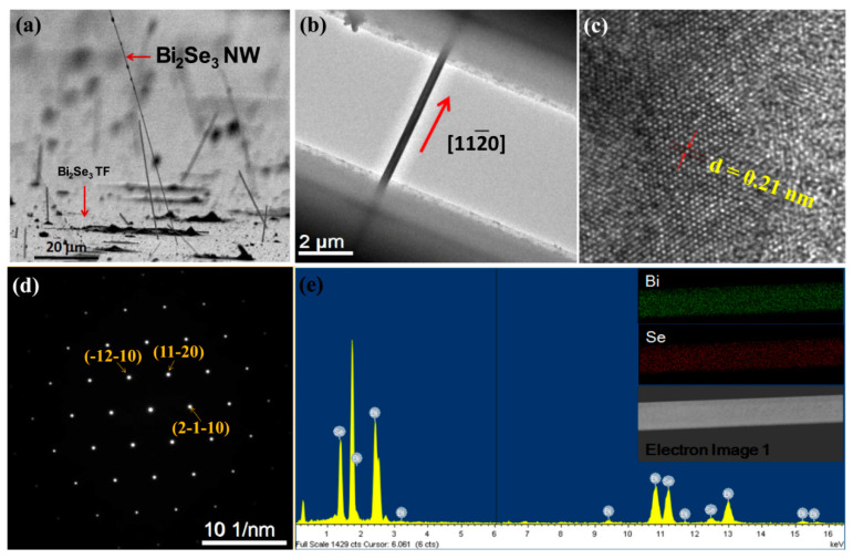
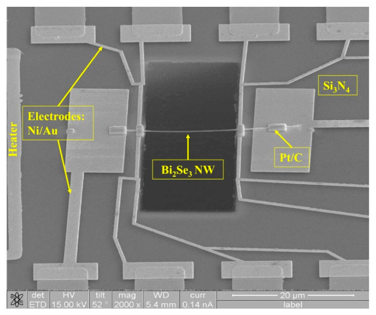
Field emission scanning electron microscopy (Hitachi Co., S-4800, Tokyo, Japan) images of the Bi2Se3 NWs (Figure 1a) showed that the NWs exhibited diameters ranging from 50 to 500 nm and lengths up to 100 µm. Straight and uniform Bi2Se3 NWs of high aspect ratio grew on the substrate after annealing. A tungsten needle (d = 100 nm) and a binocular optical microscope were used to extract a single-crystal NW from the Bi2Se3 film; the NW was then suspended on a Si3N4 microchip by using electrodes (Figure 1b) and employed in structural analyses and thermoelectricity measurements. A transmission electron microscope (TEM; JEOL JEM-2100 at 200 kV, Tokyo, Japan) was used to examine the crystalline structure of the Bi2Se3 NW (Figure 1c,d).
Figure 1.
(a) SEM image (top view) indicating that all Bi2Se3 NWs grew several micrometers in length from the surface of the Bi2Se3 TF; (b) TEM images of a single-crystal Bi2Se3 NW suspended on a Si3N4 microchip following electrode formation by using a FIB that served as the TEM holder; (c) HR-TEM image of the NW shown in (b), where the distance between crystal faces is 0.21 nm; (d) the SAED pattern (at the [0001] zone axis), confirming that the single-crystalline NWs grew in the [11,12,13,14,15,16,17,18,19,20] direction; and (e) EDS spectrum of a Bi2Se3 NW (the inset shows the EDS mapping image of a NW).
The electrical resistivity ρ and Seebeck coefficient S of the Bi2Se3 bulk were measured simultaneously using commercial equipment (ZEM-3, ULVAC-RIKO, Chigasaki, Kanagawa, Japan) in a He atmosphere from 300 to 540 K. The thermal conductivity κ of the Bi2Se3 bulk was calculated using the equation κ = D.Cp.d, where D is the thermal diffusivity, Cp is the specific heat, and d is the density of the sample. The thermal diffusivity D was examined via a laser-flash apparatus (NETZSCH, LFA 457, Selb, Germany), and the density d was obtained using the Archimedes method (presented in Figure S1, electronic supporting information (ESI)). The Seebeck coefficient S and the electrical resistivity ρ of an NW were measured using a conventional steady-state method in an Oxford cryostat. The NW thermal conductivity was measured using the 3ω method.
The TEM image (TEM; JEOL JEM-2100 at 200 kV, Tokyo, Japan) in Figure 1c reveals that the ordered hexagonal structure exhibiting lattice fringes of 0.21 nm gaps between the [11,12,13,14,15,16,17,18,19,20] planes were consistent with those of other lattice spacing measurements of Bi2Se3 NWs [47]. A corresponding selected area electron diffraction (SAED) pattern (Figure 1d) reveals that the Bi2Se3 NWs were high-quality single crystals that exhibited growth along the [11,12,13,14,15,16,17,18,19,20] direction. The chemical composition of the Bi2Se3 NW was examined using energy dispersive X-ray spectroscopy (EDS, JEOL, Tokyo, Japan); the EDS mapping shown in the inset of Figure 1e indicates the uniform spatial distribution of Bi and Se elements throughout the NW.
Figure 2 shows a SEM image of a Bi2Se3 NW (d = 200 nm) suspended on a Si3N4 microchip between 10 nm Ni/50 nm Au electrodes and a Pt/C electrical contact deposited by a focus ion beam (FIB). The sample used in this study showed nearly an ohmic contact. Subsequently, the microchip was used to determine the values of electrical resistivity ρ and S via four-point measurements.
Figure 2.
The SEM image of a single-crystal Bi2Se3 NW (diameter = 200 nm) placed on a Si3N4 microchip following electrode formation by using a FIB.
3.2. Characterization of Thermoelectric Properties
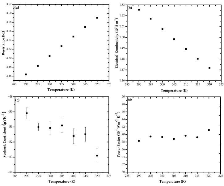
Figure 3a shows the temperature dependence of the electrical resistance at 290–320 K for a 200 nm Bi2Se3 NW that exhibited weak metallic conductivities. The σ of the NW at near room temperature was 1.50767 × 10⁵ S m−1 (Figure 3b), which was approximately 55% lower than that of the Bi2Se3 bulk single-crystal (2.7550 × 10⁵ S m−1) [41] (Table 1). Furthermore, the surface scattering of charge carriers typically yields a reduced σ value [48]. However, the σ values of the Bi2Se3 NW at room temperature was higher than those reported in previous studies on the Bi2Se3 bulk [23,24,25,26,28,29,32], and even higher than that of the Bi2Se3 single-crystal made by Hor et al. [39], probably the result of the increased contribution of conduction surfaces up to 73% of the total electrical conduction upon decreasing the NW dimension via the high surface-to-volume ratio s/v ~ 2 nm−1 of the nanowires. A previous report [19] of electrical transport experiments on Bi2Te3 and Bi2Se2Te nanowires in the range of 200–300 nm in diameter revealed that the two-dimensional TI surface channels contribute up to 30–70% of the total electrical conduction at surface-to-volume ratios of s/v = 2−5 × 10⁻² nm−1.
Figure 3.
Temperature dependence regarding the (a) electrical resistance, (b) electrical conductivity, (c) TE power (S) and (d) power factor of the single-crystal Bi2S3 NW.
Table 1.
The transport properties of Bi2Se3 nanowire and bulk at room temperature.
| Sample * | S [µV K−1] | Σ [S m−1] | PF [10−5 W m−1K−2] | κ W m−1K−1 | ZT | Ref. |
|---|---|---|---|---|---|---|
| Bi2Se3 | −53 | 38678 | 10.70 | 0.78 | 0.04 | [26] |
| Bi2Se3 | −115 | 212 | 2.80 | 0.75 | 0.01 | [28] |
| Bi2Se2.83 | −60 | 25000 | 9 | 0.55 | 0.05 | [29] |
| Bi2Se3 Nanowire SC (φ = 200 nm) | −51 | 150767 | 39.32 | 2.05 | 0.06 | Our Work |
| Bi2Se3 Bulk SC | −62.10 | 259998 | 100 | 1.55 | 0.19 | Our Work |
| Bi2Se3 Bulk SC | −190 | 47619 | 172 | 2.96 | 0.17 | [39] |
| Bi2Se3 Bulk SC | −59 | 275500 | 95.90 | 3.1 | 0.09 | [41] |
* SC = single-crystalline.
The S values with the negative sign obtained for the Bi2Se3 NW (Figure 3c) show that the Bi2Se3 NW is an n-type semiconductor, because electrons have much higher mobility than holes and dominate the transport [49,50]. This is reasonable because undoped Bi2Se3 is strongly n-type [51]. Furthermore, the room temperature S values for the n-type Bi2Se3 NW was −51 μVK−1 for the 200 nm NW, the value was comparable to those typically reported by Greenaway and Harbeke for this material (i.e., in the −55 to −73 μVK−1 range) [52], indicating that the Fermi level lay well inside the conduction band. The magnitude of the S smoothly increased as the temperature increased. This behavior was consistent with that expected of a metallically doped material. The magnitude of S for the NW tends to be zero when the temperature is decreased because S represents the entropy per electric charge and must decrease to zero at 0 K [15]. Figure 3d indicates the temperature dependence of the PF of Bi2Se3 NW, indicating that the PF increased as temperature increased; this can be attributed to the increase in the S with the temperature of the Bi2Se3 NW. The PF value of the 200 nm Bi2Se3 NW at room temperature was 39.32 × 10⁻⁵ Wm−1K−2, which was higher than the PF of the Bi2Se3 bulk nanostructures [21,22,23,24,26,27,31]. The enhanced PF value is likely a result of enhanced electronic transport of the NW.
For semiclassical transport (metals or degenerate semiconductors) the carrier-density dependence of the thermopower is described by the Mott relation [53,54,55]:
| (1) |
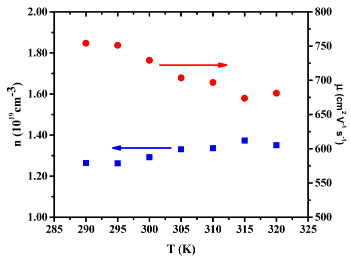
where kB is Boltzmann’s constant, q is the electron charge, h is Planck’s constant, T is the measurement temperature, m* is the effective mass of the carrier (m* = 0.14 mo in Bi2Se3) [56] and mo is the electron mass. This formula is valid for assessing metals or degenerate semiconductors that exhibit an n value in the range of 1018 to 1020 cm−3 [57,58]. The value of n is in the range of 1.26–1.35 × 1019 cm−3 at 290–320 K for the 200 nm NW (Figure 4), indicating that the NW is a degenerate semiconductor. This value is close to that calculated by Boechko et al. for n-type single crystals of a Bi2Se3 single crystal (1–4 × 1019 cm−3) [59]. The value of n increased as the temperature increased, indicating the intrinsic condition [60], with the number of thermally generated carriers exceeding the number of donor carriers. The intrinsic carrier concentration in a material ni is generally much smaller than the dopant carrier concentration at room temperature, but ni (=n·p) has a very strong temperature dependence:
| (2) |
where Eg0 is the energy band gap at T = 0 K [60].
Figure 4.
Temperature dependence of carrier concentration and carrier mobility for Bi2Se3 NW.
Figure 4 also depicts the calculated T dependences of carrier mobility μ for the Bi2Se3 NW. The μ value is obtained using the following equation:
| (3) |
Our calculated values of μ at 290–320 K were 754–681 cm2 V−1 s−1 for the 200 nm NW; these values were much smaller than those of the Bi2Se3 bulk (approximately 920–1060 cm2 V−1 s−1) [41], but higher than those reported by Le et al. [60] for Bi2Se3 TFs (7.2 ± 0.2 to 98.4 ± 0.5 cm2 V−1 s−1). The μ values decreased as temperature increased because of the phonon concentration increase that caused increased scattering. Thus, lattice scattering reduced the carrier mobility at higher temperature. The mobility of a semiconductor depends on the impurity concentrations (including donor and acceptor concentrations), defect concentration, temperature, and electron and hole concentrations.
The primary factor involved in determining μ in the semiconductor is the scattering mechanism through the relation [61]. Conduction carriers are scattered by acoustic phonons when , whereas they are scattered by ionized impurities when . The μ values of the 200 nm Bi2Se3 NW continually decreased as the T increased, indicating that phonon scattering was dominant throughout the whole temperature range.
The thermal conductivity of Bi2Se3 NW was measured by the self-heating 3ω method in the temperature range of 290–320 K. The 3ω signal can be expressed as [62,63]:
| (4) |
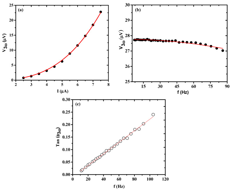
where I and ω are the amplitude and frequency of the alternating current applied on the nanowire, respectively; R and R′ are the resistance and derivative of resistance at the corresponding temperature, respectively; κ is the thermal conductivity; S is the NW cross-section area; and γ is the characteristic thermal time constant. Figure 5a shows the current dependence of V3ω at 300 K, demonstrating an I0 dependence in an intermediate current range; one can see that V3ω(I0) followed the I03 dependence well, in agreement with Equation (4). Figure 5b,c show the frequency dependencies of the amplitude and the phase angle of V3ω at 300 K, respectively, compared with the predicted functional forms (the solid lines). The fitting parameters for Figure 5a,b are shown in Tables S1 and S2, respectively.
Figure 5.
(a) The third harmonic voltage signal V3ω as function of the extraction current amplitude Io. The solid line shows the cubic relationship of V3ω and Io. (b) Frequency dependence of V3ω. The solid line is the predicted relation . (c) The frequency dependence of the phase angle of V3ω at 300 K of Bi2Se3 NW; d = 200 nm.
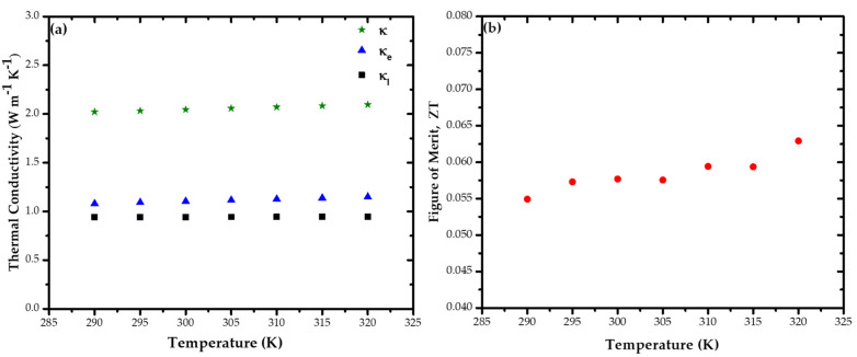
By fitting the data in Figure 5a to equation (ωγ→ 0), we obtained the thermal conductivity κ, and the thermal time constant γ was ~2 ms at 300 K, comparable to a simple theoretical calculation of κ based on the Callaway model for nanostructured Bi2Se3 made by Li et al. [64,65]. It is known that phonon-boundary scattering can suppress the thermal conductivity in nanowires [66,67]. However, the data on a Bi2Se3 NW with d = 200 nm from the experimental κ values (κ = 2.02 to 2.09 W m−1 K−1 at 290–320 K) as plotted in Figure 6a are in reasonable agreement with the Callaway model between the κ values of 300 nm (κ > 2 W m−1 K−1) and 100 nm (κ < 2 W m−1 K−1) [64]. The measured thermal conductivity, given by the κ value (κ is measured perpendicular to c plane) at T = 300 K of the NW (2.05 W m−1 K−1) was ~33% lower than those for Bi2Se3 bulk single-crystal (2.96 W m−1 K−1 or 3.1 W m−1 K−1 in Table 1) [39,41].
Figure 6.
(a) Thermal conductivity κ, and (b) figure of merit ZT values of Bi2Se3 NW in the temperature range of 290 K to 320 K.
The electronic thermal conductivity κe values of the Bi2Se3 NWs here were calculated according to the Wiedemann–Franz law:
| κe = LσT | (5) |
where L is the Lorenz number (2.44 × 10⁻⁸ W Ω K−2). When subtracting the κe values from the measured thermal conductivity, one obtains the phonon (or lattice) part of the thermal conductivity as κl = κ-κe. The temperature-dependent data for κl thus obtained are shown in Figure 6a. The obtained for κl and κe at 300 K for NWs were 29% and 37% lower than that of the Bi2Se3 bulk single-crystal (κl = 1.33 W m−1 K−1 and κe = 1.77 W m−1 K−1) [41]. The thermal conductivity was dominated by the electronic contribution in the 290–320 K range, although Birkholz and Rosi both reported a value for κl of Bi2Se3 bulk of between 2.0 and 2.4 W m−1 K−1 [51]. It was shown that the large surface-to-volume ratio s/v of nanowires could enhance phonon surface scattering and decrease κl.
Additionally, for this nanowire, ZT calculated from the obtained S, σ, and κ was approximately 0.06 at 300 K (Figure 6b). However, the ZT values of this nanowire were still higher than those of Bi2Se3 bulk used to construct nanostructures at 290–320 K, as reported previously [26,28,29]. Table 1 shows a summary of the transport properties of single-crystalline Bi2Se3 NW, compared with those reported Bi2Se3 bulk at room temperature. Our S, σ, and κ results of Bi2Se3 NW d = 200 nm were in reasonable agreement with a theoretical study [19]. This agreement indicates the high-quality crystallinity of the Bi2Se3 NWs grown by the stress-induced method.
4. Conclusions
The stress-induced method was applied to grow single-crystalline Bi2Se3 nanowires (NWs) from a Bi2Se3 TF on a SiO2/Si substrate, offering an alternative technique for Bi2Se3 NWs synthesis without a catalyst. This technique had not been previously applied to Bi2Se3 alloys. In this work, at room temperature, the Bi2Se3 nanowire (NW) (d = 200 nm) exhibited a PF of approximately 39.32 × 10⁻⁵ Wm−1K−2, which was higher than that reported for Bi2Se3 bulk nanostructures; this discrepancy was mainly attributed to the electron-transport contribution of this NW. The measured thermal conductivity κ value of a NW was 2.05 W m−1 K−1, which was 31−34% lower than those for a Bi2Se3 bulk single crystal [39,41] because of the electron-scattering contribution. The figure of merit ZT value of Bi2Se3 NW rose up to approximately 0.06 at room temperature, in agreement with a theoretical study of the thermoelectric properties on a topological insulator of Bi2Se3 NWs [19]. Our results indicated that NWs grown using the stress-induced method yield high-quality single crystals.
Acknowledgments
The authors wish to thank the Core Facilities for Nanoscience and Nanotechnology at the Institute of Physics of the Academia Sinica in Taiwan for providing technical support.
Supplementary Materials
The following are available online at https://www.mdpi.com/2079-4991/11/3/819/s1, Figure S1: (a) Image of Bi2Se3 single-crystalline grown by the Bridgman method. (b) The measured thermoelectric properties were −62.10 μ VK−1, 259998 S m−1, 1.55 W m−1 K−1, and 0.19 for the Seebeck coefficient (S), electrical conductivity (σ), thermal conductivity (κ) and figure of merit ZT, respectively, at room temperature, as shown in Table 1, Table S1: The fitting parameters of the third harmonic voltage signal V3ω as function of the extraction current amplitude Io for Figure 5a, Table S2: The fitting parameters of frequency dependence of V3ω for Figure 5b.
Author Contributions
Conceptualization, D. and Y.-Y.C.; methodology, D., P.-C.W. and P.-C.L.; software, D. and P.-C.L.; validation, D. and Y.-Y.C.; formal analysis, D., P.-C.L. and Y.-Y.C.; investigation, D., P.-C.L. and Y.-Y.C.; resources, D., P.-C.W. and P.-C.L.; data curation, D., P.-C.L. and Y.-Y.C.; writing—original draft preparation, D.; writing—review and editing, D., P.-C.L. and Y.-Y.C.; visualization, D.; project administration, P.-C.L. and Y.-Y.C.; supervision, Y.-Y.C.; funding acquisition, D. and Y.-Y.C., All authors have read and agreed to the published version of the manuscript.
Funding
This study was funded by the National Science Council of Taiwan (grant NSC 100-2112-M-001-019-MY3), and the publishing fee was supported by the Research Center for Electronics and Telecommunications (P2ET), Indonesian Institute of Sciences (LIPI).
Data Availability Statement
The data presented in this study are available on request from the corresponding author.
Conflicts of Interest
The authors declare no conflict of interest.
Footnotes
Publisher’s Note: MDPI stays neutral with regard to jurisdictional claims in published maps and institutional affiliations.
References
- 1.Boukai A.I., Bunimovich Y., Tahir-Kheli J., Yu J.K., Goddard W.A., Heath J.R. Silicon nanowires as efficient thermoelectric materials. Nature. 2008;451:168–171. doi: 10.1038/nature06458. [DOI] [PubMed] [Google Scholar]
- 2.Bubnova O., Khan Z.U., Malti A., Braun S., Fahlman M., Berggren M., Crispin X. Optimization of the thermoelectric figure of merit in the conducting polymer poly(3,4-ethylenedioxythiophene) Nat. Mater. 2011;10:429–433. doi: 10.1038/nmat3012. [DOI] [PubMed] [Google Scholar]
- 3.Hochbaum A.I., Chen R., Delgado R.D., Liang W., Garnett E.C., Najarian M., Majumdar A., Yang P. Enhanced thermoelectric performance of rough silicon nanowires. Nature. 2008;451:163–167. doi: 10.1038/nature06381. [DOI] [PubMed] [Google Scholar]
- 4.Minnich A.J., Dresselhaus M.S., Ren Z.F., Chen G. Bulk nanostructured thermoelectric materials: Current research and future prospects. Energy Environ. Sci. 2009;2:466–479. doi: 10.1039/b822664b. [DOI] [Google Scholar]
- 5.Zhao H., Pokheral M., Zhu G., Chen S., Lukas K., Jie Q., Opeil C., Chen G., Ren Z. Dramatic thermal conductivity reduction by nanostructures for large increase in thermoelectric figure-of-merit of FeSb2. Appl. Phys. Lett. 2011;99:2012–2015. doi: 10.1063/1.3651757. [DOI] [Google Scholar]
- 6.Snyder G.J., Toberer E.S. Complex thermoelectric materials. Mater. Sustain. Energy Collect. Peer Rev. Res. Rev. Artic. Nat. Publ. Group. 2010;7:101–110. doi: 10.1038/nmat2090. [DOI] [PubMed] [Google Scholar]
- 7.Tritt T.M., Subramanian M.A. Thermoelectric Materials, Phenomena and Applications: A Bird’s Eye View. MRS bulletin. 2006;31:188–198. doi: 10.1557/mrs2006.44. [DOI] [Google Scholar]
- 8.Disalvo F.J. Thermoelectric cooling and power generation. Science. 1999;285:703–706. doi: 10.1126/science.285.5428.703. [DOI] [PubMed] [Google Scholar]
- 9.Tritt T.M. Thermoelectric materials:Holey and Unholey Semiconductors. Science. 1999;283:804–805. doi: 10.1126/science.283.5403.804. [DOI] [Google Scholar]
- 10.Rowe D.M. CRC Handbook of Thermoelectrics. CRC Press; Danvers, MA, USA: 1995. [Google Scholar]
- 11.Dresselhaus M.S., Chen G., Tang M.Y., Yang R., Lee H., Wang D., Ren Z., Fleurial J.P., Gogna P. New directions for low-dimensional thermoelectric materials. Adv. Mater. 2007;19:1043–1053. doi: 10.1002/adma.200600527. [DOI] [Google Scholar]
- 12.Mahan G.D., Sofo J.O. The best thermoelectric. Proc. Natl. Acad. Sci. USA. 1996;93:7436–7439. doi: 10.1073/pnas.93.15.7436. [DOI] [PMC free article] [PubMed] [Google Scholar]
- 13.Lin Y.M., Sun X., Dresselhaus M. Theoretical investigation of thermoelectric transport properties of cylindrical Bi nanowires. Phys. Rev. B. 2000;62:4610–4623. doi: 10.1103/PhysRevB.62.4610. [DOI] [Google Scholar]
- 14.Hicks L., Dresselhaus M.S. Effect of quantum-well structures on the thermoelectric figure of merit. Phys. Rev. B. 1993;47:12727. doi: 10.1103/PhysRevB.47.12727. [DOI] [PubMed] [Google Scholar]
- 15.Boukai A., Xu K., Heath J.R. Size-dependent transport and thermoelectric properties of individual polycrystalline bismuth nanowires. Adv. Mater. 2006;18:864–869. doi: 10.1002/adma.200502194. [DOI] [Google Scholar]
- 16.Slack G. CRC Handbok Thermoelectrics. CRC Press; Danvers, MA, USA: 1995. New Materials and Performance Limits for Thermoelectric Cooling. [Google Scholar]
- 17.Mishra S.K., Satpathy S., Jepsen O. Electronic structure and thermoelectric properties of bismuth telluride and bismuth selenide. J. Phys. Condens. Matter. 1997;9:461–470. doi: 10.1088/0953-8984/9/2/014. [DOI] [Google Scholar]
- 18.Al Bayaz A., Giani A., Foucaran A., Pascal-Delannoy F., Boyer A. Electrical and thermoelectrical properties of Bi2Se3 grown by metal organic chemical vapour deposition technique. Thin Solid Films. 2003;441:1–5. doi: 10.1016/S0040-6090(03)00675-8. [DOI] [Google Scholar]
- 19.Gooth J., Gluschke J.G., Zierold R., Leijnse M., Linke H., Nielsch K. Thermoelectric performance of classical topological insulator nanowires. Semicond. Sci. Technol. 2015;30:015015. doi: 10.1088/0268-1242/30/1/015015. [DOI] [Google Scholar]
- 20.Watanabe K., Sato N., Miyaoka S. New optical recording material for video disc system. J. Appl. Phys. 1983;54:1256–1260. doi: 10.1063/1.332188. [DOI] [Google Scholar]
- 21.Waters J., Crouch D., Raftery J., O’Brien P. Deposition of bismuth chalcogenide thin films using novel single-source precursors by metal-organic chemical vapor deposition. Chem. Mater. 2004;16:3289–3298. doi: 10.1021/cm035287o. [DOI] [Google Scholar]
- 22.Venkatasubramanian R., Siivola E., Colpitts T., O’Quinn B. Thin-film thermoelectric devices with high room-temperature figures of merit. Nature. 2001;413:597–602. doi: 10.1038/35098012. [DOI] [PubMed] [Google Scholar]
- 23.Xu H., Chen G., Jin R., Pei J., Wang Y., Chen D. Hierarchical Bi2Se3 microrods: Microwave-assisted synthesis, growth mechanism and their related properties. Cryst. Eng. Comm. 2013;15:1618–1625. doi: 10.1039/c2ce26678d. [DOI] [Google Scholar]
- 24.Xu H., Chen G., Jin R., Chen D., Wang Y., Pei J., Zhang Y., Yan C., Qiu Z. Microwave-assisted synthesis of Bi2Se3 ultrathin nanosheets and its electrical conductivities. Cryst. Eng. Comm. 2014;16:3965–3970. doi: 10.1039/C4CE00004H. [DOI] [Google Scholar]
- 25.Lin Y.F., Chang H.W., Lu S.Y., Liu C.W. Preparation, characterization, and electrophysical properties of nanostructured BiPO4 and Bi2Se3 derived from a structurally characterized, single-source precursor Bi[Se2P(OiPr)2]3. J. Phys. Chem. C. 2007;111:18538–18544. doi: 10.1021/jp076886b. [DOI] [Google Scholar]
- 26.Bai T., Li C., Liang D., Li F., Jin D., Shi Z., Feng S. Synthesis of various metal selenide nanostructures using the novel selenium precursor 1,5-bis(3-methylimidazole-2-selone)pentane. Cryst. Eng. Comm. 2013;15:6483–6490. doi: 10.1039/c3ce40491a. [DOI] [Google Scholar]
- 27.Manjare S.T., Yadav S., Singh H.B., Butcher R.J. Redox reaction between main-group elements (Te, Sn, Bi) and N-Heterocyclic-carbene-derived selenium halides: A facile method for the preparation of monomeric halides. Eur. J. Inorg. Chem. 2013;2013:5344–5357. doi: 10.1002/ejic.201300850. [DOI] [Google Scholar]
- 28.Kadel K., Kumari L., Li W.Z., Huang J.Y., Provencio P.P. Synthesis and thermoelectric properties of Bi2Se3 nanostructures. Nanoscale Res. Lett. 2011;6:57. doi: 10.1007/s11671-010-9795-7. [DOI] [PMC free article] [PubMed] [Google Scholar]
- 29.Min Y., Roh J.W., Yang H., Park M., Kim S.I., Hwang S., Lee S.M., Lee K.H., Jeong U. Surfactant-free scalable synthesis of Bi2Te3 and Bi2Se3 nanoflakes and enhanced thermoelectric properties of their nanocomposites. Adv. Mater. 2013;25:1425–1429. doi: 10.1002/adma.201203764. [DOI] [PubMed] [Google Scholar]
- 30.Sun Z., Liufu S., Chen L. Synthesis and characterization of nanostructured bismuth selenide thin films. Dalt. Trans. 2010;39:10883–10887. doi: 10.1039/c0dt00840k. [DOI] [PubMed] [Google Scholar]
- 31.Giani A., Al Bayaz A., Foucaran A., Pascal-Delannoy F., Boyer A. Elaboration of Bi2Se3 by metalorganic chemical vapour deposition. J. Cryst. Growth. 2002;236:217–220. doi: 10.1016/S0022-0248(01)02095-4. [DOI] [Google Scholar]
- 32.Alegria L.D., Schroer M.D., Chatterjee A., Poirier G.R., Pretko M., Patel S.K., Petta J.R. Structural and electrical characterization of Bi 2Se 3 nanostructures grown by metal-organic chemical vapor deposition. Nano Lett. 2012;12:4711–4714. doi: 10.1021/nl302108r. [DOI] [PubMed] [Google Scholar]
- 33.Sun Y., Cheng H., Gao S., Liu Q., Sun Z., Xiao C., Wu C., Wei S., Xie Y. Atomically thick bismuth selenide freestanding single layers achieving enhanced thermoelectric energy harvesting. J. Am. Chem. Soc. 2012;134:20294–20297. doi: 10.1021/ja3102049. [DOI] [PubMed] [Google Scholar]
- 34.Checkelsky J.G., Hor Y.S., Cava R.J., Ong N.P. Bulk band gap and surface state conduction observed in voltage-tuned crystals of the topological insulator Bi2Se3. Phys. Rev. Lett. 2011;106:4–7. doi: 10.1103/PhysRevLett.106.196801. [DOI] [PubMed] [Google Scholar]
- 35.Hong S.S., Kundhikanjana W., Cha J.J., Lai K., Kong D., Meister S., Kelly M.A., Shen Z.X., Cui Y. Ultrathin topological insulator Bi2Se3 nanoribbons exfoliated by atomic force microscopy. Nano Lett. 2010;10:3118–3122. doi: 10.1021/nl101884h. [DOI] [PubMed] [Google Scholar]
- 36.Janíček P., Drašar Č., Beneš L., Lošták P. Thermoelectric properties of Tl-doped Bi2Se3 single crystals. Cryst. Res. Technol. 2009;44:505–510. doi: 10.1002/crat.200800615. [DOI] [Google Scholar]
- 37.King M.D., Blanton T.N., Misture S.T., Korter T.M. Prediction of the unknown crystal structure of creatine using fully quantum mechanical methods. Cryst. Growth Des. 2011;11:5733–5740. doi: 10.1021/cg2013599. [DOI] [Google Scholar]
- 38.Kašparová J., Drašar Č., Krejčová A., Beneš L., Lošt’ák P., Chen W., Zhou Z., Uher C. n-type to p-type crossover in quaternary Bi xSb yPb zSe 3 single crystals. J. Appl. Phys. 2005;97:103720. doi: 10.1063/1.1904158. [DOI] [Google Scholar]
- 39.Hor Y.S., Richardella A., Roushan P., Xia Y., Checkelsky J.G., Yazdani A., Hasan M.Z., Ong N.P., Cava R.J. P-type Bi2Se3 for topological insulator and low-temperature thermoelectric applications. Phys. Rev. B. 2009;79:195208. doi: 10.1103/PhysRevB.79.195208. [DOI] [Google Scholar]
- 40.Qiu X., Austin L.N., Muscarella P.A., Dyck J.S., Burda C. Nanostructured Bi2Se3 films and their thermoelectric transport properties. Angew. Chem. Int. Ed. 2006;45:5656–5659. doi: 10.1002/anie.200600848. [DOI] [PubMed] [Google Scholar]
- 41.Navrátil J., Horák J., Plecháček T., Kamba S., Lošt’ák P., Dyck J.S., Chen W., Uher C. Conduction band splitting and transport properties of Bi2Se3. J. Solid State Chem. 2004;177:1704–1712. doi: 10.1016/j.jssc.2003.12.031. [DOI] [Google Scholar]
- 42.Dedi, Lee P.C., Chien C.H., Dong G.P., Huang W.C., Chen C.L., Tseng C.M., Harutyunyan S.R., Lee C.H., Chen Y.Y. Stress-induced growth of single-crystalline lead telluride nanowires and their thermoelectric transport properties. Appl. Phys. Lett. 2013;103:1–6. doi: 10.1063/1.4813606. [DOI] [Google Scholar]
- 43.Dedi, Chien C.H., Hsiung T.C., Chen Y.C., Huang Y.C., Lee P.C., Lee C.H., Chen Y.Y. Structural, electronic transport and magnetoresistance of a 142nm lead telluride nanowire synthesized using stress-induced growth. AIP Adv. 2014;4:1–7. doi: 10.1063/1.4876919. [DOI] [Google Scholar]
- 44.Cheng Y.T., Weiner A.M., Wong C.A., Balogh M.P., Lukitsch M.J. Stress-induced growth of bismuth nanowires. Appl. Phys. Lett. 2002;81:3248–3250. doi: 10.1063/1.1515885. [DOI] [Google Scholar]
- 45.Shim W., Ham J., Lee K., Jeung W.Y., Johnson M., Lee W. On-film formation of Bi nanowires with extraordinary electron mobility. Nano Lett. 2009;9:18–22. doi: 10.1021/nl8016829. [DOI] [PubMed] [Google Scholar]
- 46.Chen X., Zhou H.D., Kiswandhi A., Miotkowski I., Chen Y.P., Sharma P.A., Lima Sharma A.L., Hekmaty M.A., Smirnov D., Jiang Z. Thermal expansion coefficients of Bi2Se3 and Sb2Te3 crystals from 10 K to 270 K. Appl. Phys. Lett. 2011;99:12–15. doi: 10.1063/1.3672198. [DOI] [Google Scholar]
- 47.Kong D., Randel J.C., Peng H., Cha J.J., Meister S., Lai K., Chen Y., Shen Z.X., Manoharan H.C., Cui Y. Topological insulator nanowires and nanoribbons. Nano Lett. 2010;10:329–333. doi: 10.1021/nl903663a. [DOI] [PubMed] [Google Scholar]
- 48.Wang D., Sheriff B.A., Heath J.R. Complementary symmetry silicon nanowire logic: Power-efficient inverters with gain. Small. 2006;2:1153–1158. doi: 10.1002/smll.200600249. [DOI] [PubMed] [Google Scholar]
- 49.Partin D.L. Growth and characterization of epitaxial bismuth films. J. Vac. Sci. Technol. B Microelectron. Nanom. Struct. 1989;7:348. doi: 10.1116/1.584748. [DOI] [Google Scholar]
- 50.De Kuijper A.H., Bisschop J. Temperature dependence of concentrations and mobilities in thin bismuth films. Thin Solid Films. 1983;110:99–106. doi: 10.1016/0040-6090(83)90214-6. [DOI] [Google Scholar]
- 51.Nolas G.S., Sharp J., Goldsmid J. Thermoelectrics: Basic Principles and New Materials Developments. Volume 45. Springer-Verlag; Berlin/Heidelberg, Germany: 2013. [Google Scholar]
- 52.Greenaway D.L., Harbeke G. Band structure of bismuth telluride, bismuth selenide and their respective alloys. J. Phys. Chem. Solids. 1965;26:1585–1604. doi: 10.1016/0022-3697(65)90092-2. [DOI] [Google Scholar]
- 53.Dedi, Idayanti N., Lee P.-C., Lee C.-H., Chen Y.-Y. Thermoelectric power of single crystalline lead telluride nanowire. J. Phys. Conf. Ser. 2016;776:012046. doi: 10.1088/1742-6596/776/1/012046. [DOI] [Google Scholar]
- 54.Kim D., Syers P., Butch N.P., Paglione J., Fuhrer M.S. Ambipolar surface state thermoelectric power of topological insulator Bi2Se3. Nano Lett. 2014;14:1701–1706. doi: 10.1021/nl4032154. [DOI] [PubMed] [Google Scholar]
- 55.Cutler M., Mott N.F. Observation of anderson localization in an electron gas. Phys. Rev. 1969;181:1336–1340. doi: 10.1103/PhysRev.181.1336. [DOI] [Google Scholar]
- 56.Wang Z., Lin T., Wei P., Liu X., Dumas R., Liu K., Shi J. Tuning carrier type and density in Bi2Se3 by Ca-doping. Appl. Phys. Lett. 2010;97:2012–2015. doi: 10.1063/1.3473778. [DOI] [Google Scholar]
- 57.Horák J., Navrátil J., Starý Z. Lattice point defects and free-carrier concentration in Bi2+xTe3 and Bi2+xSe3 crystals. J. Phys. Chem. Solids. 1992;53:1067–1072. doi: 10.1016/0022-3697(92)90079-S. [DOI] [Google Scholar]
- 58.Lee C.H., Yi G.C., Zuev Y.M., Kim P. Thermoelectric power measurements of wide band gap semiconducting nanowires. Appl. Phys. Lett. 2009;94:1–4. doi: 10.1063/1.3067868. [DOI] [Google Scholar]
- 59.Wolpert D., Ampadu P. Managing Temperature Effects in Nanoscale Adaptive Systems. Volume XXII. Springer-Verlag; New York, NY, USA: 2012. pp. 1–174. Hardcover. [Google Scholar]
- 60.Le P.H., Liao C.N., Luo C.W., Lin J.Y., Leu J. Thermoelectric properties of bismuth-selenide films with controlled morphology and texture grown using pulsed laser deposition. Appl. Surf. Sci. 2013;285:657–663. doi: 10.1016/j.apsusc.2013.08.107. [DOI] [Google Scholar]
- 61.Sze S.M., Ng K.K. Physics of Semiconductor Devices. 3rd ed. Wiley; Danvers, MA, USA: 2007. [Google Scholar]
- 62.Lu L., Yi W., Zhang D.L. 3 Ω method for specific heat and thermal conductivity measurements. Rev. Sci. Instrum. 2001;72:2996–3003. doi: 10.1063/1.1378340. [DOI] [Google Scholar]
- 63.Dedi, Primadona I., Lee P.C., Chien C.H., Chen Y.Y. Structural and Thermoelectric Properties Characterization of Individual Single-Crystalline Nanowire. In: Shahzad A., editor. Impact of Thermal Conductivity on Energy Technologies. IntechOpen; London, UK: 2018. pp. 149–166. [Google Scholar]
- 64.Li G., Liang D., Qiu R.L.J., Gao X.P.A. Thermal conductivity measurement of individual Bi2Se3 nano-ribbon by self-heating three-ω method. Appl. Phys. Lett. 2013;102:043104. doi: 10.1063/1.4789530. [DOI] [Google Scholar]
- 65.Callaway J. Model for lattice thermal conductivity at low temperatures. Phys. Rev. 1959;113:1046–1051. doi: 10.1103/PhysRev.113.1046. [DOI] [Google Scholar]
- 66.Zhou J., Jin C., Seol J.H., Li X., Shi L. Thermoelectric properties of individual electrodeposited bismuth telluride nanowires. Appl. Phys. Lett. 2005;87:133109. doi: 10.1063/1.2058217. [DOI] [Google Scholar]
- 67.Li D., Wu Y., Kim P., Shi L., Yang P., Majumdar A. Thermal conductivity of individual silicon nanowires. Appl. Phys. Lett. 2003;83:2934–2936. doi: 10.1063/1.1616981. [DOI] [Google Scholar]
Associated Data
This section collects any data citations, data availability statements, or supplementary materials included in this article.
Supplementary Materials
Data Availability Statement
The data presented in this study are available on request from the corresponding author.


