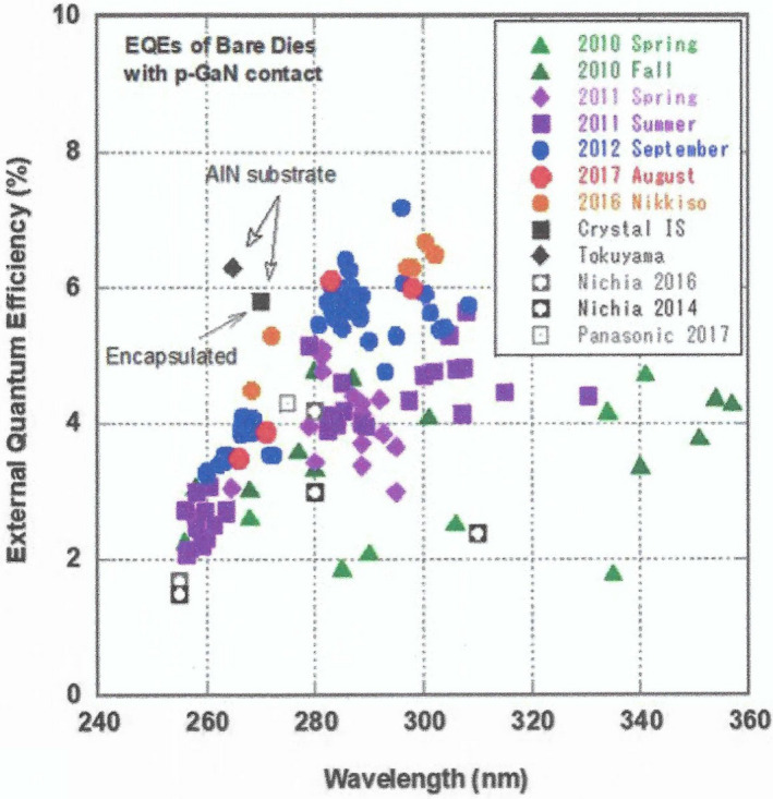
Figure 4.

FEQE mapping of AlGaN‐based LED dies with p‐GaN contact layer. The data are mainly for LED dies on planar sapphire from our group (colored). EQEs of LED dies from elsewhere (uncolored) using AlN substrates and sapphire substrates with a p‐GaN contact layer are also shown. Solid uncolored symbols indicate the use of an AlN bulk substrate, where “_” indicates with encapsulation and “u” indicates no encapsulation. The EQEs in the case of an AlN substrate (“_” and “u”) were achieved with a roughened light extraction surface. Uncolored open marks represent LED dies with p‐GaN layer fabricated on planar sapphire reported by other groups. All of our data (colored) were obtained without boosting light extraction efficiency (LEE) using encapsulation or a sapphire lens (9).
