Figure 3.
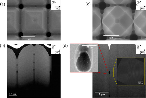
TEM cross sections of 5 μm tall Si microcrystals, grown at 720 °C and partially merged with the neighboring ones. The crystals are cut along the red lines in the SEM images during the TEM lamella preparation. (a) Microcrystals grown at a rate of 5 nm/s where a single pit is visible in the top view SEM image. (b) Two separate arrays of regularly spaced voids are visible, one at the center of the crystals and one in the merging region. (c) Merged microcrystals grown at a rate of 1.25 nm/s where no pit is visible in the top view SEM image. (d) TEM cross section of one nanovoid in the merging region between two crystals grown at 1.25 nm/s. The STEM LAADF image (red inset) shows well-defined facets, while no dislocations are observed near the void in the STEM WBDF image (yellow inset).

