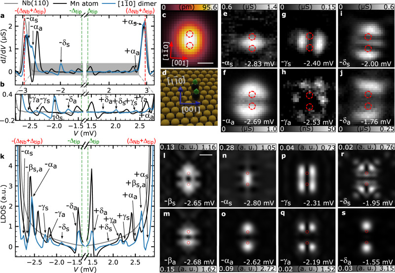
Fig. 2. Hybridized Shiba states in a FM-coupled Mn dimer.
a dI/dV spectrum taken between the two atoms of a dimer (blue) with reference spectra for the substrate (gray) and a single Mn adatom (black). b Magnification of the spectra shown in panel a. Shiba states are labeled and marked by arrows. Vertical lines mark sample and tip gaps. c Small-scale STM image of a Mn dimer. The white scale bar has a length of 500 pm (Vbias =6 mV and I=1 nA). The directions and the scale bar also apply to panels e–j. d 3D rendered illustration of the positions of the two Mn adatoms (black spheres) in the investigated dimer with respect to the Nb substrate atoms (yellow spheres), including the spin structure indicated by green arrows. e–j dI/dV maps measured on the dimer in the same area shown in panel c for the given bias voltages where a peak/shoulder is visible in the spectrum in a and b. The dI/dV maps taken at the Shiba peaks on the positive bias side are shown in Supplementary Fig. 6. LDOS calculated between the two atoms of the FM-aligned dimer (blue), on a single adatom (black) and on the bare superconductor (gray) convoluted with the DOS of the superconducting tip. l–s Calculated two-dimensional maps of the LDOS at the indicated bias voltages. The white scale bar has a length of 500 pm; crystallographic directions as in panel c. Red circles in c, e–j and l–s denote the locations of the Mn adatoms in the dimer.

