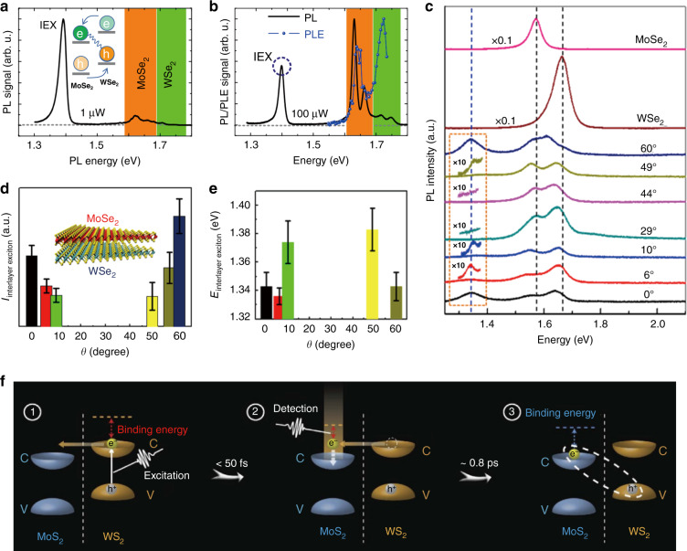
Fig. 2. Interlayer exciton formation in TMD vdW heterostructures.
a PL spectrum of the MoSe2/WSe2 heterostructure measured at 4.5 K with 1 μW excitation power28. IEX represents the emissions from interlayer excitons. b PL spectrum of the MoSe2/WSe2 heterostructure (black line) measured at 4.5 K with 100 μW excitation power and the PLE spectrum (blue dots) of the interlayer exciton emission (IEX, marked by the blue dashed circle)28. c PL spectra of the MoSe2 monolayer, WSe2 monolayer, and MoSe2/WSe2 heterobilayer for various twist angles (0° ≤ θ ≤ 60°) at room temperature101. d, e Twist-angle-dependent PL intensity (d) and energy (e) of the interlayer excitons formed in MoSe2/WSe2 heterobilayers101. f Illustration of the interlayer exciton formation process in MoS2/WS2 heterostructures as revealed by transient absorption spectroscopy55. a, b Reprinted with permission from ref. 28 [IOP Publishing]. c–e Reprinted with permission from ref. 101 [American Chemical Society]. f Reprinted with permission from ref. 55 [Springer Nature Limited]

