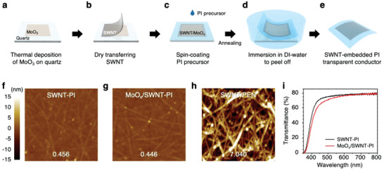
Figure 1.

Fabrication of the ultrathin SWNT–PI conductor. a–e) Schematic illustration of the fabrication process of SWNT–PI ultrathin conductors: a) thermal deposition of MoO3 on a quartz glass substrate, b) dry transfer of SWNT film, c) spin‐coating of PI precursor and annealing to cure the PI film and p‐dope the SWNTs with MoOx, d) lifting off of the SWNT–PI conductor from the glass substrate, and e) the resulting ultrathin transparent conductor. AFM topography images of f) SWNT–PI, g) MoOx/SWNT–PI, and h) SWNT/PEN substrates (area: 1.5 × 1.5 µm2, rms roughness values are displayed on each image), and i) optical transmittance spectra of the SWNT–PI‐based films.
