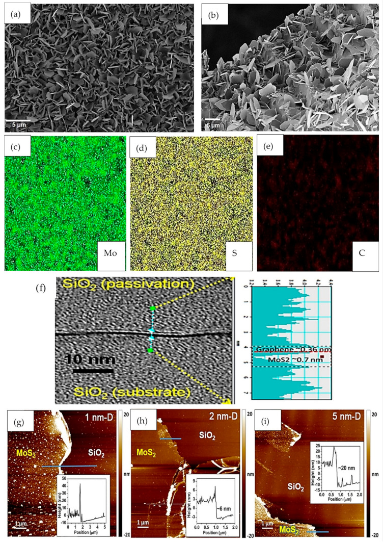
Figure 8.
(a,b) Vertically grown MoS2 nanosheet on graphene, (c–e) EDS elementary mapping of vertical MoS2 (element of mapping is mentioned in the bottom right corner) (Republished with permission of Royal Society of Chemistry, from [59]; permission conveyed through Copyright Clearance Center, Inc., 2019), (f) high resolution TEM (HRTEM) image of graphene/heterostructures with thicknesses extracted from the intensity profile (Reproduced with permission from [32], Published by Springer Nature, 2014) and atomic force microscope (AFM) images of MoS2 films on SiO2/Si substrate with pre-deposited Mo thicknesses of (g) 1 nm, (h) 2 nm and (i) 5 nm (Reprinted from [9], with permission from Elsevier, 2018).

