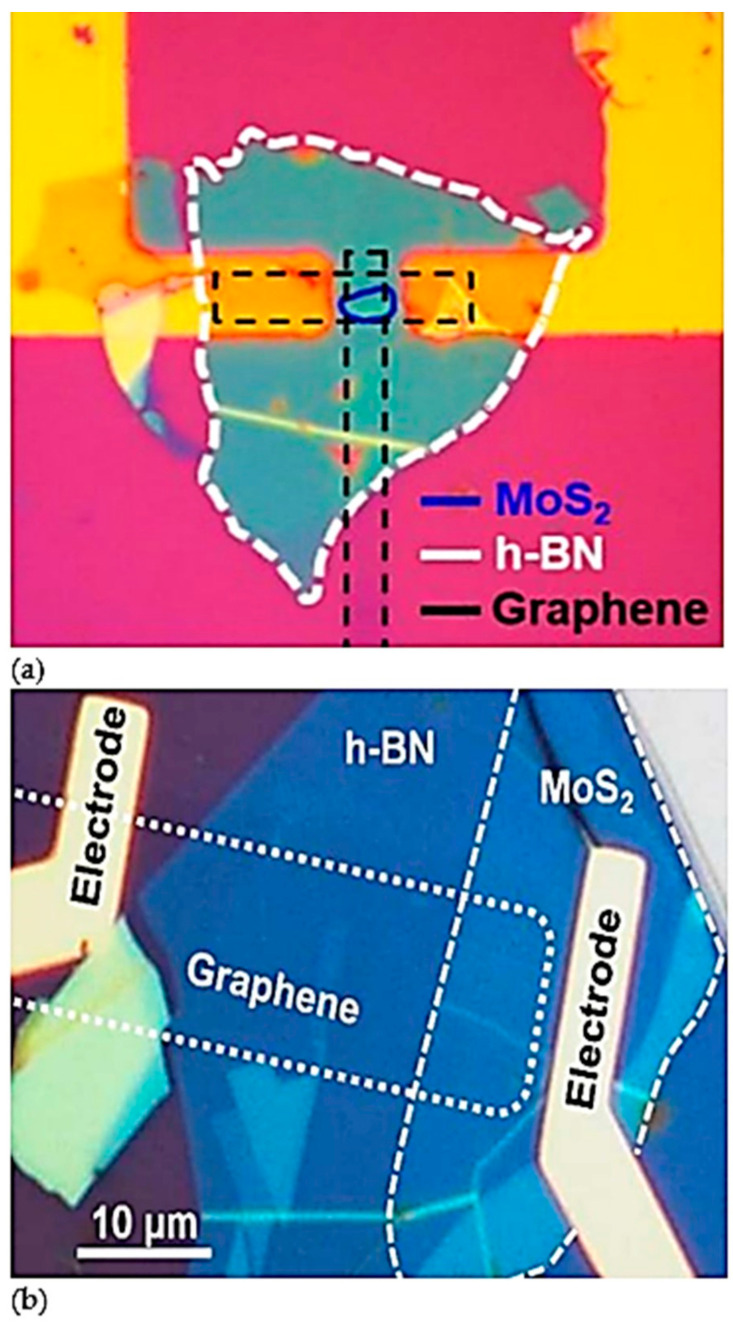
Figure 9.
Optical images of MoS2/h-BN/graphene heterostructures. (a) Lateral graphene/MoS2/graphene device with channel length of 30 nm. h-BN serves as the dielectric layer for transparent graphene gate electrode (Reprinted with permission from [19], American Chemical Society, 2020). and (b) The dotted line is graphene layer at the bottom, the dashed line is monolayer of MoS2 at the top and 11 nm thick h-BN layer between them (Reprinted with permission from [47], American Chemical Society, 2017).

