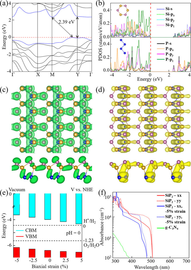
Figure 3.

(a) Electronic band structure of the SiP2 monolayer. The horizontal dashed line is the VBM. (b) PDOS of the P and Si atoms in the Si3P3 honeycombs and the P atoms in the zigzag P chains. Top and side views of the charge densities at the (c) VBM and (d) CBM. (e) Energetic positions of the VBM and CBM under biaxial strain. The dashed lines mark the redox potentials of water at pH = 0. (f) Optical absorption coefficient of the SiP2 monolayer compared to g-C3N4.
