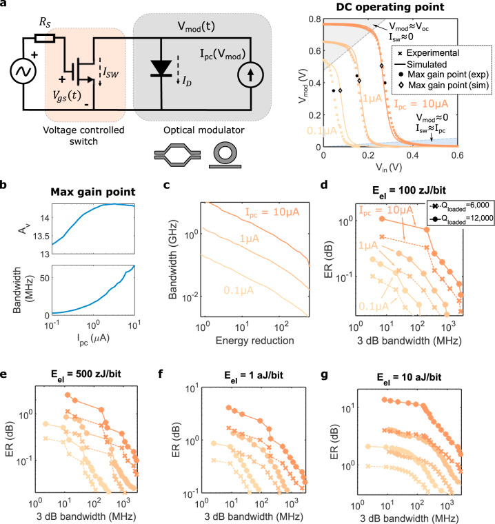
Fig. 3. Photovoltaic modulator model and simulated performance.
a Large signal model of a photovoltaic (PV) modulator. By controlling the current flowing through the transistor (Isw) via the gate voltage (Vgs) we can switch the voltage at the modulator terminals (Vmod) between 0 and the open-circuit voltage of the device Voc. Simulation (lines) and experimental (crosses) data is shown. Diamonds and circles highlight the bias point resulting in maximum gain. b Voltage gain Aν (top) and bandwidth (bottom) at the maximum gain point as a function of photogenerated current (Ipc). c Achievable bandwidth as a function of the reduction in electrical energy consumption compared to conventional modulation, calculated using Eq. (1). Cmod = 20 fF and Cg is calculated as outlined in Supplementary Discussion 4. d–g Extinction ratio (ER) as a function of 3 dB bandwidth in a PV modulator for four different electrical energy consumptions (Eel). Crosses correspond to a Lorentzian resonance with a loaded quality factor Qloaded = 6000, and dots to Qloaded = 12,000. The maximum insertion loss of the modulation is limited to 6 dB in all plots. Different colors correspond to different generated photocurrents as indicated in (d).

